Recessed-type field effect transistor with reduced body effect

a field effect transistor and recessed-type technology, applied in the direction of transistors, electrical devices, semiconductor devices, etc., can solve the problems of undesired body effects, reduced channel length of the transistor, and inability to prevent undesired body effects, etc., to achieve stable threshold voltage, prevent body effects, and stable operation

Inactive Publication Date: 2005-08-11
SAMSUNG ELECTRONICS CO LTD
View PDF5 Cites 38 Cited by
  • Summary
  • Abstract
  • Description
  • Claims
  • Application Information

AI Technical Summary

Benefits of technology

[0012] In an example application, the field effect transistor is formed as part of a DRAM (dynamic random access memory) cell. In that case, the respective line pad disposed on the source is coupled to a storage capacitor of the DRAM cell, and the gate electrode forms a word line for the DRAM cell. However, the field effect transistor of the present invention may be applied for other types of integrated circuits.
[0013] In this manner, because the extra-doped channel region abuts the gate insulator at walls of the opening of the recessed type field effect transistor, body effect is prevented. Thus, the field effect transistor has a more stable threshold voltage for more stable operation.

Problems solved by technology

However, undesired short-channel effects result in the field effect transistor from such reduced channel length.
However, the anti-punch through layer in Wu is formed well below the opening such that the field effect transistor of Wu is still susceptible to undesired body effect.
In Wu, the anti-punch through layer does not abut the walls of the opening such that the anti-punch through layer does not prevent the undesired body effect.

Method used


Image

  • Recessed-type field effect transistor with reduced body effect
  • Recessed-type field effect transistor with reduced body effect
  • Recessed-type field effect transistor with reduced body effect

Examples


Embodiment Construction

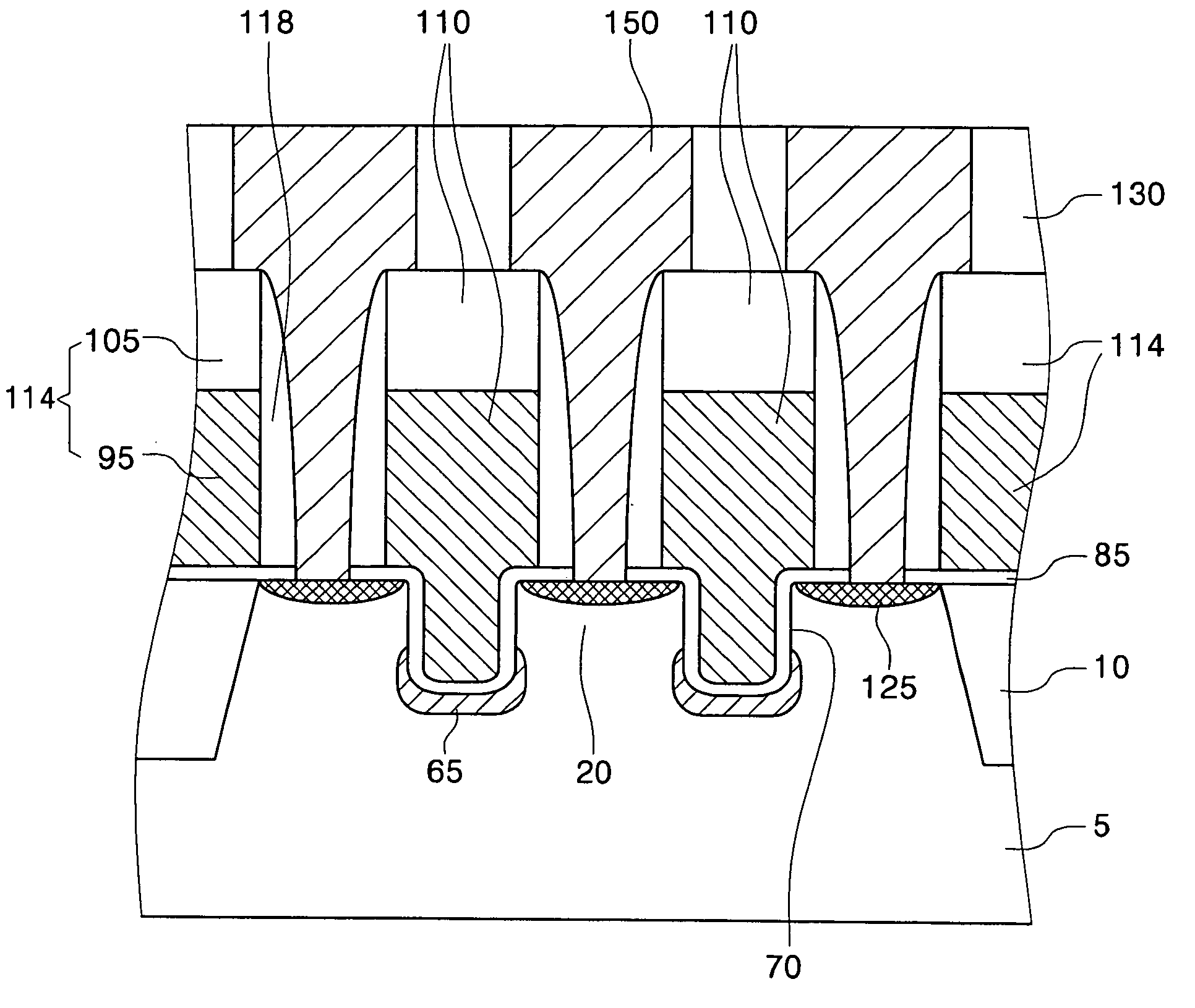
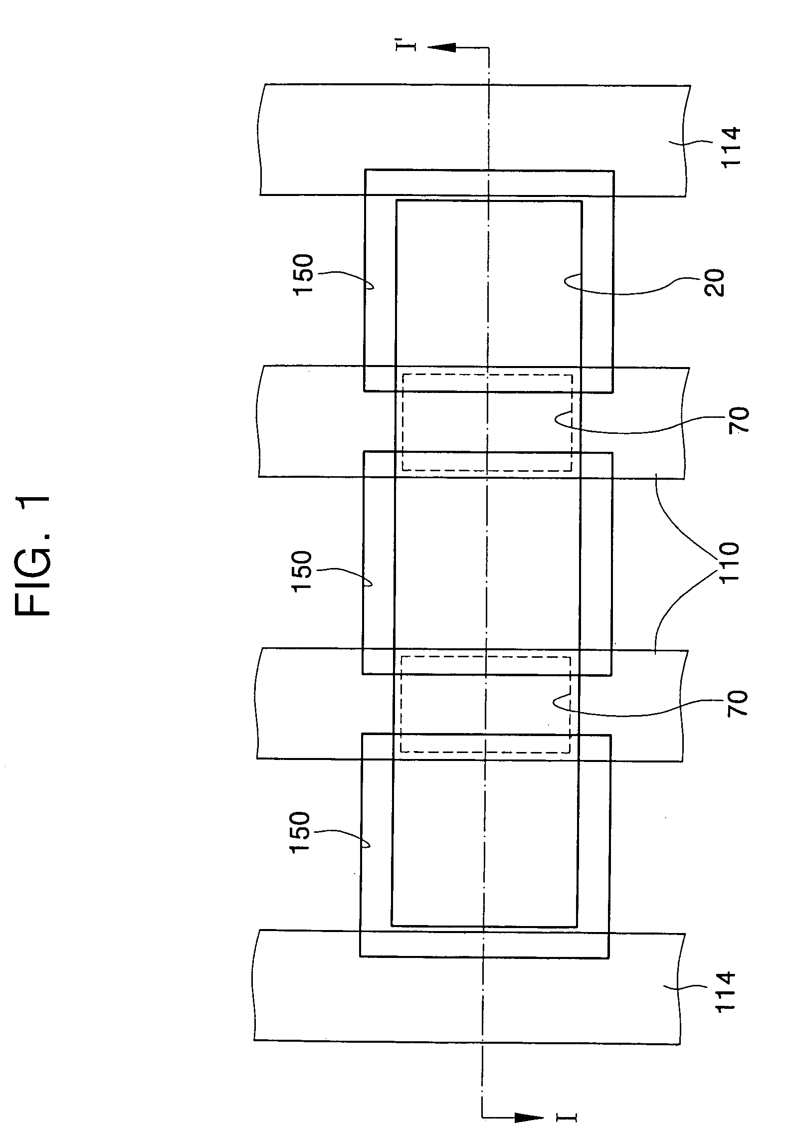
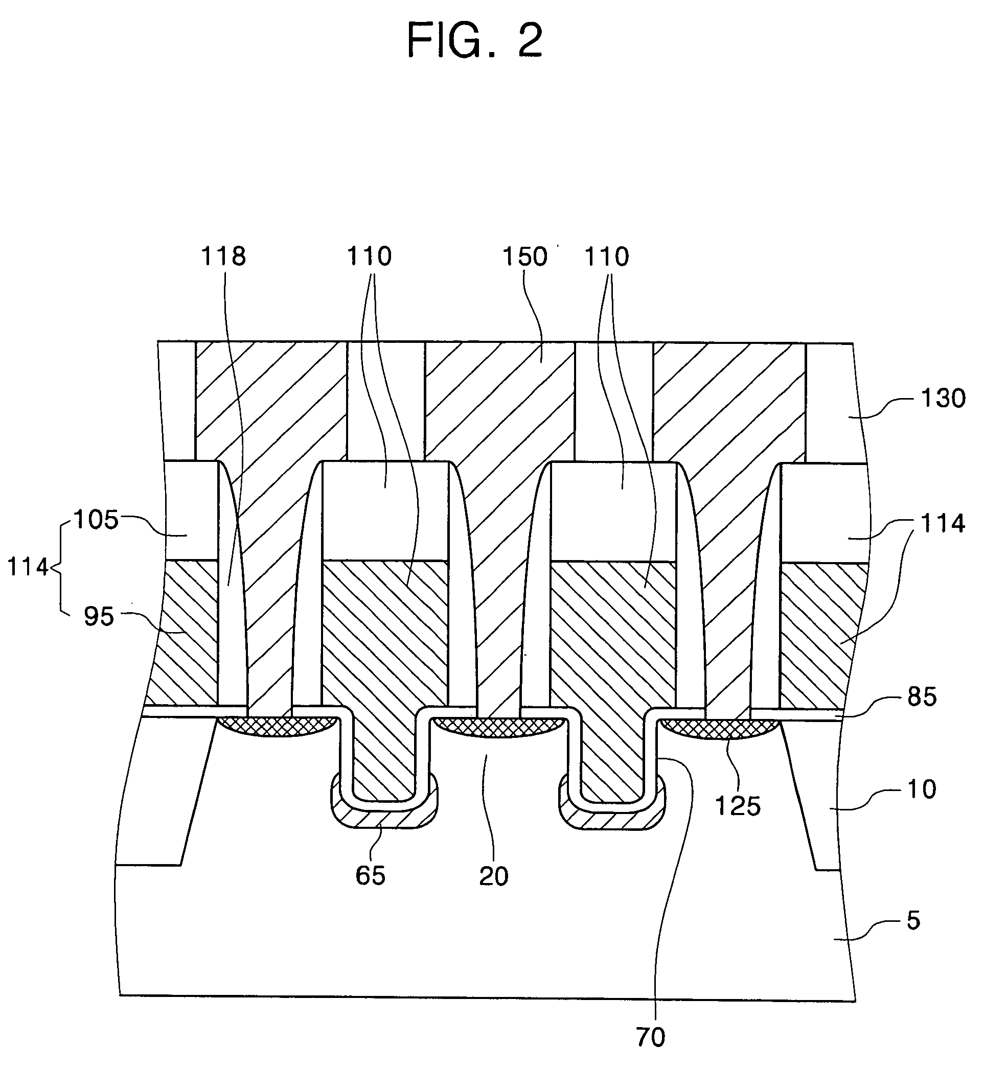
[0020]FIG. 1 shows a layout of field effect transistors formed according to an embodiment of the present invention. FIG. 2 shows a cross-sectional view of such field effect transistors along line I-I′ of FIG. 1.

[0021] Referring to FIGS. 1 and 2, a STI (shallow trench isolation) structure 10 is formed within a semiconductor substrate 5 to define an active region 20. The STI structure 10 is comprised of an insulating material such as silicon dioxide (SiO2), and the semiconductor substrate 5 is comprised of a semiconductor material such as silicon. At least one opening 70 is formed into the semiconductor substrate 5 within the active region 20. The openings 70 each have a trench shape in one embodiment of the present invention.

[0022] Each opening 70 has a gate insulator 85 formed at walls including a bottom wall and side walls of the opening 70. In addition, an extra-doped channel region 65 is formed to surround a bottom portion of each opening 70. For example, the extra-doped channe...


PUM


Abstract

For fabricating a field effect transistor, an extra-doped channel region is formed below a surface of a semiconductor substrate. An opening is formed in the semiconductor substrate into the extra-doped channel region. A gate insulator is formed at walls of the opening such that the extra-doped channel region abuts the gate insulator at a bottom portion of the opening. The opening is filled with a gate electrode. Such an extra-doped channel region prevents undesired body effect in the field effect transistor.

Description

BACKGROUND OF THE INVENTION [0001] This patent application claims priority to Korean Patent Application No. 2004-0009122, filed on Feb. 11, 2004 in the Korean Intellectual Property Office, the disclosure of which is hereby incorporated by reference in its entirety. 1. FIELD OF THE INVENTION [0002] The present invention relates generally to integrated circuit fabrication, and more particularly to fabrication of a recessed-type field effect transistor with an extra-doped channel region to reduce body effect. 2. DESCRIPTION OF THE RELATED ART [0003] Field effect transistors are a common component of many integrated circuits. A field effect transistor includes a source and a drain for defining a channel region, a gate insulator, and a gate electrode. The structure and operation of a field effect transistor is by now well known to one of ordinary skill in the art of electronics. [0004] As device dimensions are constantly scaled down, the channel length of the field effect transistor is c...

Claims


Application Information

Patent Timeline
Patent Type & Authority Applications(United States)
IPC IPC(8): H01L21/336H01L21/8234H01L21/8242H01L29/10H01L29/423
CPCH01L21/823437H01L21/823487H01L27/10852H01L29/66621H01L29/1041H01L29/42376H01L29/66537H01L27/10876H10B12/033H10B12/053H01L21/18
Inventor KIM, DONG-HYUNSONG, DU-HEONLEE, SANG-HYUNSEO, HYEOUNG-WONWON, DAE-JOONG
Owner SAMSUNG ELECTRONICS CO LTD
Why Eureka
Try Eureka