

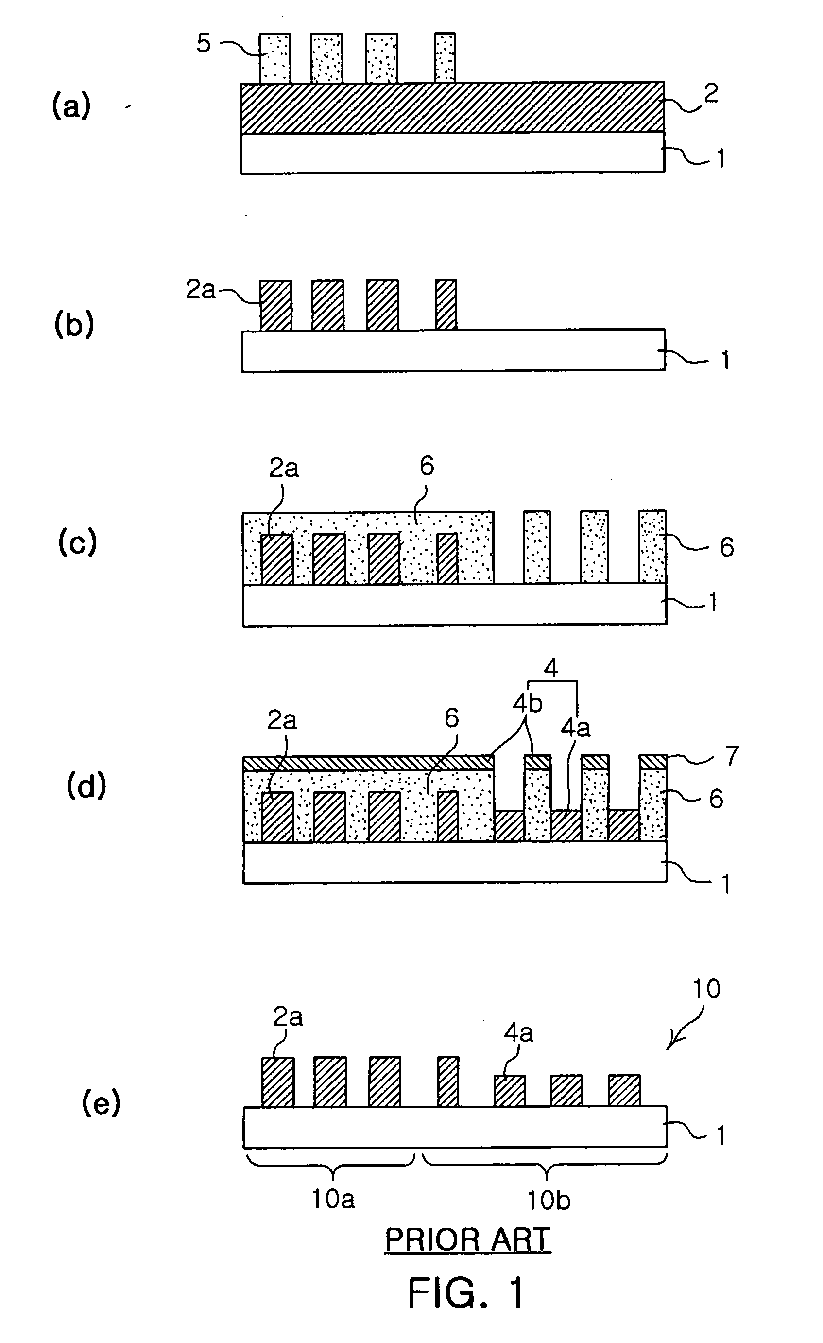
Fabrication method of multiple band surface acoustic wave devices
a surface acoustic wave and fabrication method technology, applied in the direction of electrical transducers, transducer types, electric/electrostrictive transducers, etc., can solve the problems of degrading the side profile the photoresist pattern step can rarely produce a clean side profile in the pattern, and the unsatisfactory problems of the photoresist pattern, etc., to achieve the effect of preventing damage to the surface of the pi
- Summary
- Abstract
- Description
- Claims
- Application Information
AI Technical Summary
Benefits of technology
Problems solved by technology
Method used
Image

Examples
Embodiment Construction
[0022] Preferred embodiments of the present invention will now be described in detail with reference to the accompanying drawings.
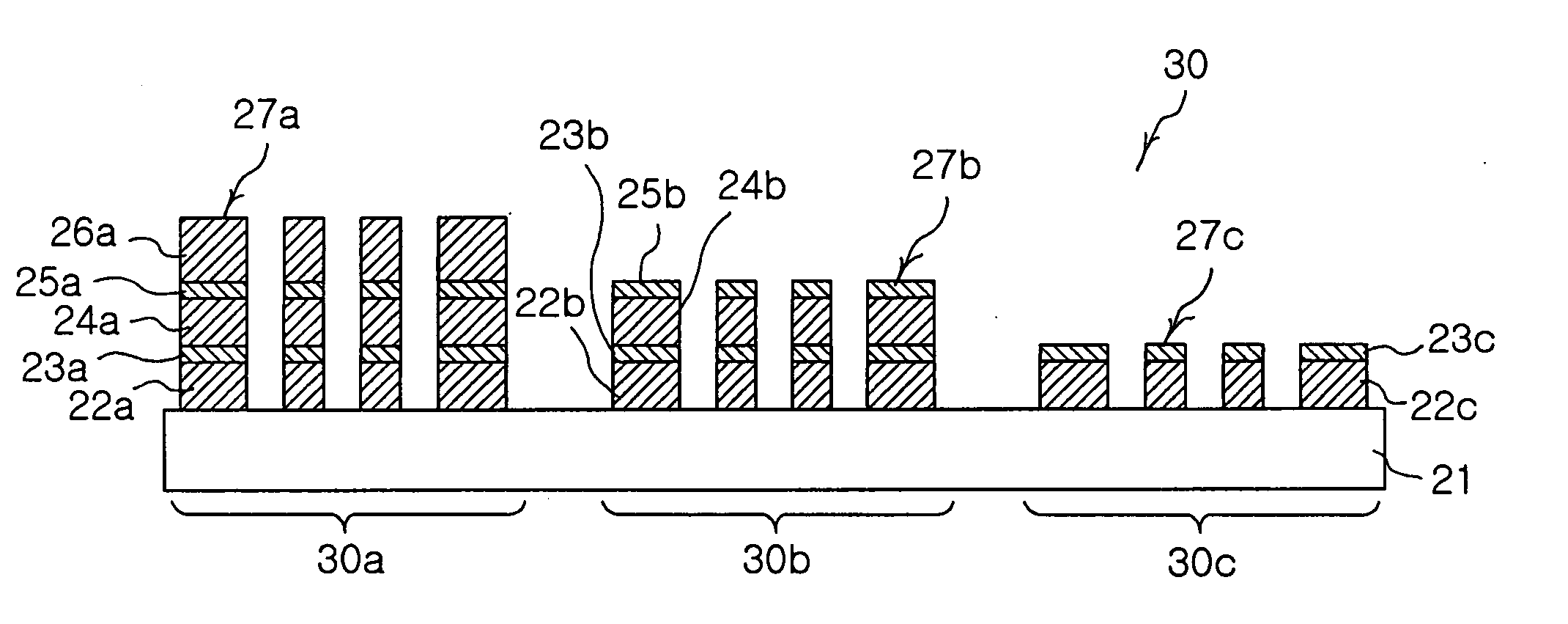
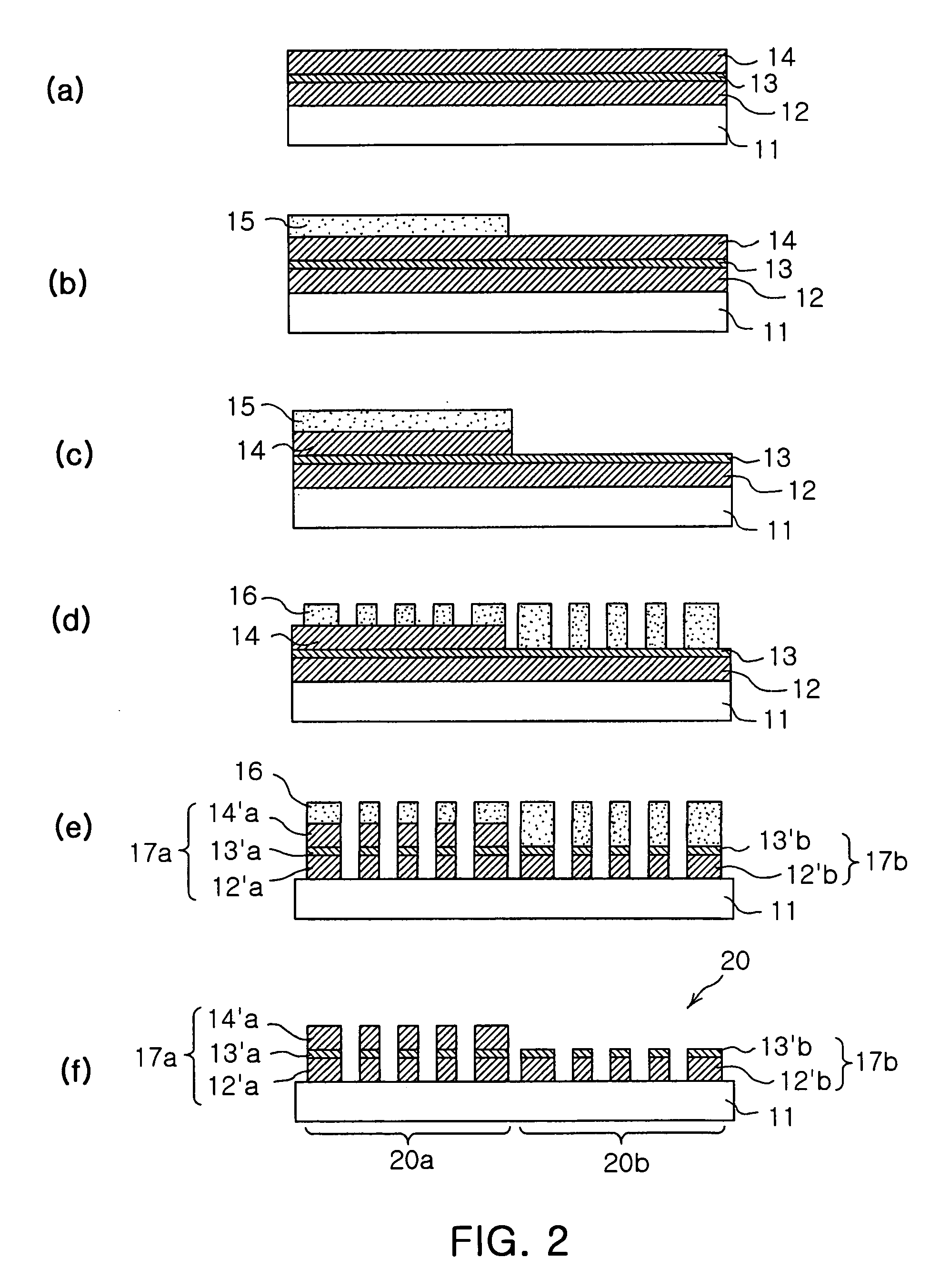
[0023]FIGS. 2A to 2F are stepwise sectional views illustrating a fabrication method of SAW devices according to the invention, which provides a SAW device having first and second SAW filters of different electrode thickness formed on a single piezoelectric ceramic substrate.
[0024] First, as shown in FIG. 2A, a first conductive layer 12, an etch-stop layer 13 and a second conductive layer 14 are formed one atop another in their order on a piezoelectric ceramic substrate 11. The piezoelectric ceramic substrate 11 may be made of for example LiTaO2 or LiNbO2, and the etch-stop layer 13 is made of a conductive material with its etching rate showing a great difference at least from that of the first conductive layer 12 according to etching conditions. Preferably, the first conductive layer 12 is made of for example Al that is a typical electrode material for ...
PUM
| Property | Measurement | Unit |
|---|---|---|
| thickness | aaaaa | aaaaa |
| thickness | aaaaa | aaaaa |
| conductive | aaaaa | aaaaa |
Abstract
Description
Claims
Application Information