Method for expanding a trench in a semiconductor structure

a technology of semiconductor structure and trench, applied in the direction of semiconductor devices, electrical equipment, basic electric elements, etc., can solve the problems of hsub>2/sub>o rinsing giving rise to problems, consumption of siosub>2/sub>, etc., and achieve the effect of improving the control of the etching process

Inactive Publication Date: 2005-08-11
POLARIS INNOVATIONS LTD
View PDF6 Cites 33 Cited by
  • Summary
  • Abstract
  • Description
  • Claims
  • Application Information

AI Technical Summary

Benefits of technology

[0022] The present invention provides an improved method for expanding a trench in a semiconductor structure in which the etching process can be better controlled.
[0025] The method according to the invention makes it possible to stop the etching process without changing the pH of the etching chemical. The SiO2 stabilized by NH3 can be removed by comparatively rapid diffusion from the trench. Only afterward is the rinsing with H2O effected.
[0026] The present invention thus makes it possible to decouple the etching process from the concentration of the reactive species by stopping the etching by means of an anodic current pulse which brings about an oxide passivation of the silicon surfaces.
[0032] In accordance with a further preferred embodiment, the trench is expanded in the lower region and is masked in the upper region by means of an insulation collar for protection against the expansion.

Problems solved by technology

The H2O rinsing gives rise to problems, however, in so far as dissolved SiO2 precipitates as silica gel as a result of the negative pH shift of the water rinsing and forms complexes which can outdiffuse significantly more slowly than protons of the water rinsing can indiffuse.
The disadvantage consists in the consumption of SiO2, that is to say also in an attack on the insulation collar 120.

Method used


Image

  • Method for expanding a trench in a semiconductor structure
  • Method for expanding a trench in a semiconductor structure
  • Method for expanding a trench in a semiconductor structure

Examples


Embodiment Construction

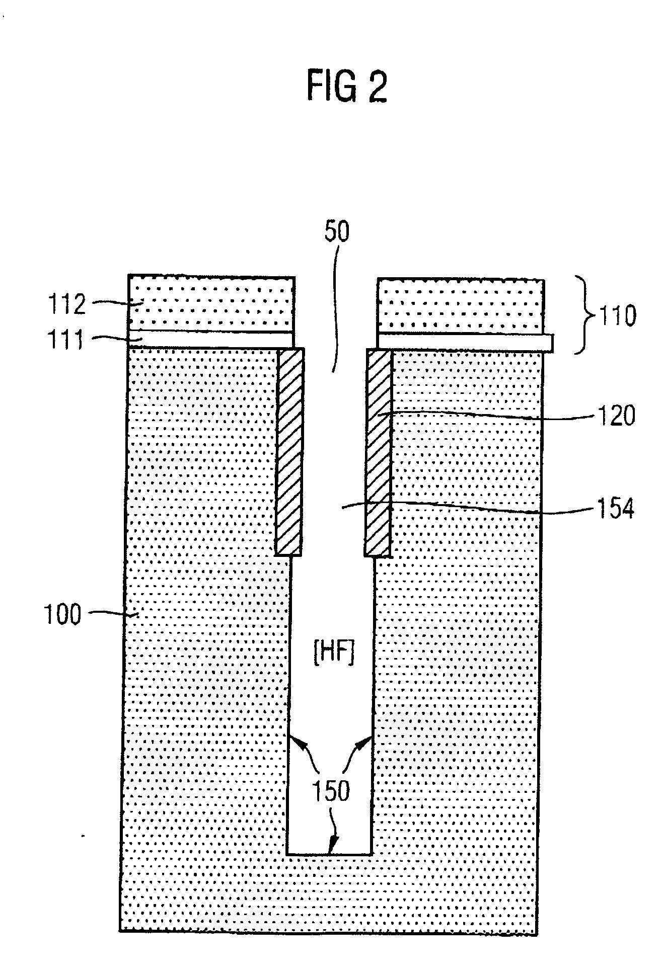
[0041] The embodiment of the present invention begins with the process steps in accordance with FIGS. 2 and 3 that have already been described above.

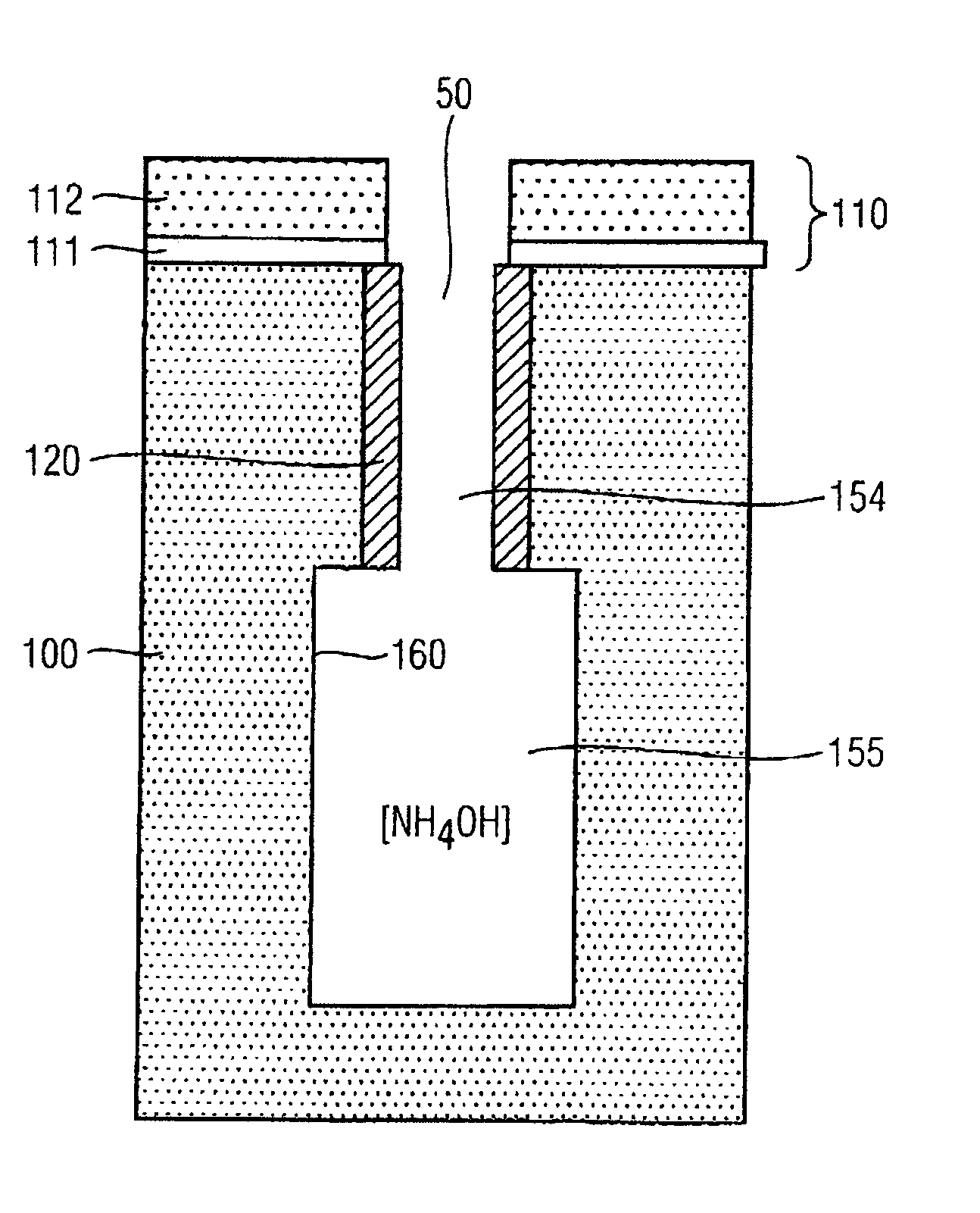
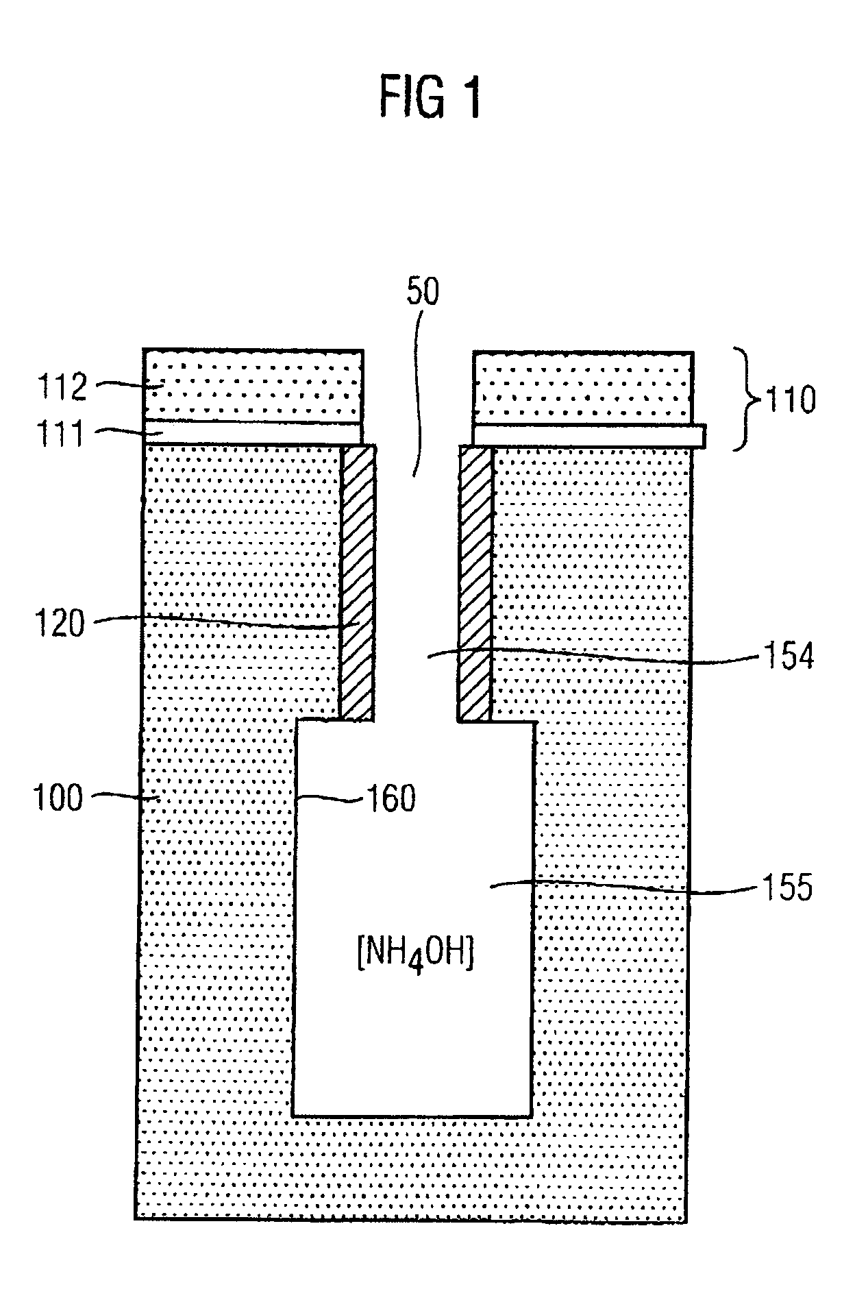
[0042] In contrast to the known process explained comprehensively above, in the case of the process according to the invention, after the trench 50 has been expanded by means of the alkaline NH4OH etching, an anodic passivation of the uncovered silicon surfaces by means of an SiO2 layer 160 is performed. The alkaline stabilized SiO2 can subsequently pass out of the trench 50 by diffusion before a negative pH shift occurs as a result of rinsing with water.

[0043] The anodic passivation is achieved for example by treating the relevant wafer in a single wafer reactor and applying to it an electrical potential which can be applied by means of a rear side contact, on the one hand, and by means of an inert electrode dipped into the etching solution, on the other hand.

[0044] The described etching process according to the invention typically ...


PUM


Abstract

The present invention provides a method for expanding a trench in a semiconductor structure. A trench is provided in a semiconductor substrate, hydrogen-terminated silicon surfaces are provided in the trench, anisotropic wet etching of the silicon surfaces in the trench with an alkaline etchant occur, and the trench is rinsed with a proton-containing neutralizing agent for the removal of the alkaline etchant. Between the wet etching step and the rinsing step, an anodic passivation of the etched silicon surfaces in the trench is carried out, in the course of which an etching stop layer is formed on the etched silicon surfaces in the trench.

Description

CLAIM FOR PRIORITY [0001] This application claims the benefit of priority to German Application No. 10 2004 006 545.4, filed in the German language on Feb. 10, 2004, the contents of which are hereby incorporated by reference. TECHNICAL FIELD OF THE INVENTION [0002] The present invention relates to a method for expanding a trench in a semiconductor structure. BACKGROUND OF THE INVENTION [0003] Although applicable to arbitrary semiconductor structures, the present invention and also the problem area on which it is based are explained on the basis of trenches for storage capacitors in semiconductor memory devices. [0004] Modern semiconductor memory devices have trench capacitors in order that the individual memory cells comprising the trench capacitor and an associated selection transistor have a least possible space requirement. [0005] Since the capacitance of a trench capacitor is directly proportional to its surface area, the trenches of the trench capacitors are usually expanded by...

Claims


Application Information

Patent Timeline
Patent Type & Authority Applications(United States)
IPC IPC(8): H01L21/306H01L21/8242
CPCH01L27/1087H01L21/30604H10B12/0387
Inventor KUDELKA, STEPHAN
Owner POLARIS INNOVATIONS LTD
Why Eureka
Try Eureka