Method and system for identifying and locating defects in an integrated circuit

a technology of integrated circuits and defects, applied in the direction of testing circuits, resistance/reactance/impedence, instruments, etc., can solve the problems of circuits that have internal shorts, are defective, circuits that are defective, etc., and achieve the effect of reducing the effect of contact resistan

Inactive Publication Date: 2005-08-18
PLUSQUELLIC JAMES FRANCIS
View PDF2 Cites 29 Cited by
  • Summary
  • Abstract
  • Description
  • Claims
  • Application Information

AI Technical Summary

Benefits of technology

[0008] There is further provided a method for reducing the effect of contact resistance from test probe connections, comprising determining a first array of reference calibration power signal values for a reference device, determining a second array of test device power signal values for the integ

Problems solved by technology

As packaging adds significant cost to the final product, the die is ordinarily tested after fabrication is completed but before packaging to determine whether it is defective, in which case it is not packaged.
If the total quiescent current significantly exceeds the maximum expected amoun

Method used


Image

  • Method and system for identifying and locating defects in an integrated circuit
  • Method and system for identifying and locating defects in an integrated circuit
  • Method and system for identifying and locating defects in an integrated circuit

Examples


Embodiment Construction

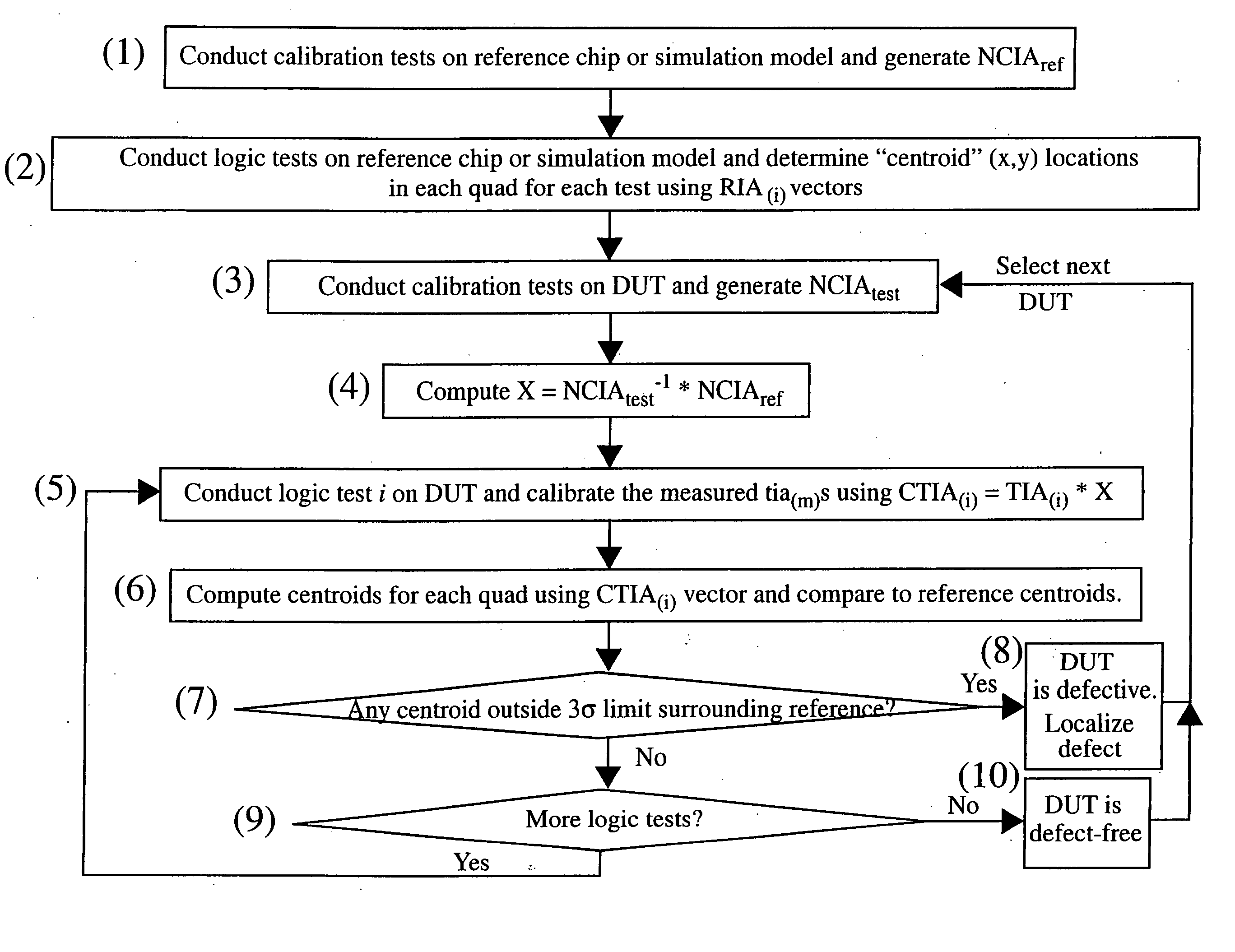
[0023] The present invention comprises a method and system for testing integrated circuits (“IC”s), particularly large-scale digital ICs, during production, after the circuit die, or chip, has been fabricated but before it is packaged. The invention takes advantage of the dynamic response of the power grid of the IC device under test (“DUT”) both to determine whether the DUT is defective and, if so, to locate the defect. To provide useful terminology and to assist in understanding the description of the invention herein, it is useful first to describe some pertinent features of a typical IC that the invention may be used to test.

1. Typical Integrated Circuit Structure

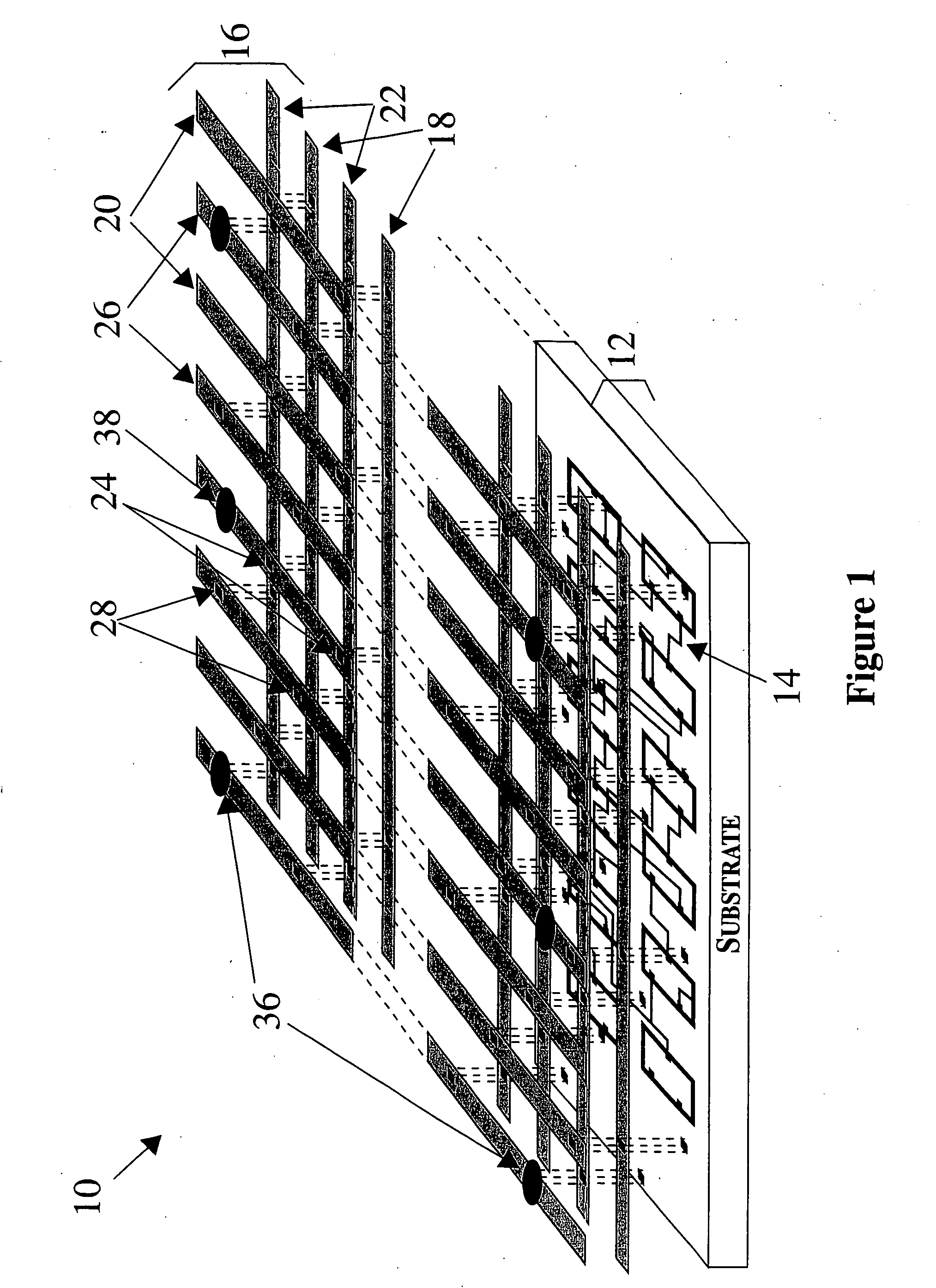
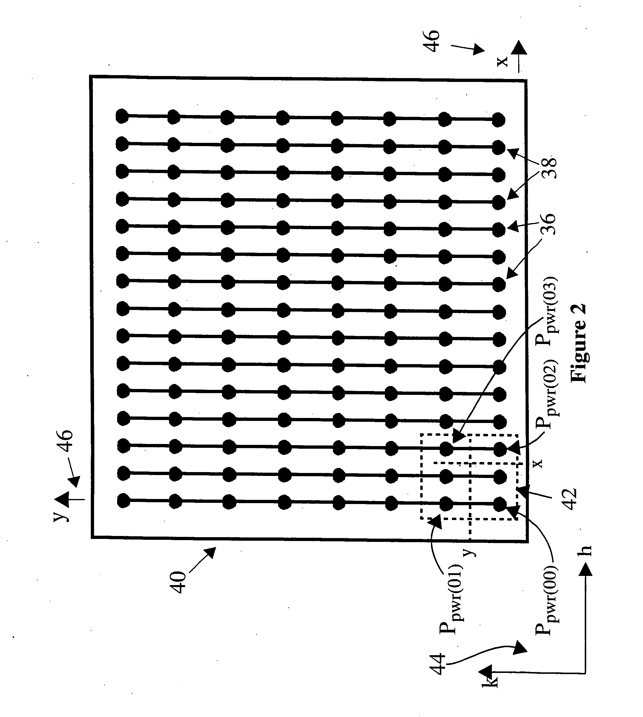
[0024] Referring to FIG. 1, a typical IC die 10 includes a substrate 12, on which circuit devices such as transistors, resistors and capacitors are formed, signal routing conductors 14, and a three-dimensional power distribution conductor network, or power grid, 16. The power grid includes layers of metallic conducto...


PUM


Abstract

A method and system for detecting and locating defects in an integrated circuit. A time-varying input signal is applied to the integrated circuit, power signals produced at a plurality of respective ordered connections in response to the input signal are measured, and one or more defects in the integrated circuit are identified from the power signals so measured. A system is provided having a probe for connecting to the die of an integrated circuit prior to final packaging, a testing system for applying transient input signals to the die and acquiring die power signal measurements in response thereto, and a data processor for determining whether the power signal measurements indicate the presence of a defect in the die. Also provided is a method for reducing the effect of contact resistance from test probe connections. As a way of implementing the approach of the method and system there is also provided an integrated circuit having a plurality of ordered connections to the power grid and a plurality of calibration circuits associated with respective ordered connections so as to selectively inject transient signals onto the power grid at respective locations.

Description

BACKGROUND OF THE INVENTION [0001] This invention relates to production testing of integrated circuits, particularly production testing of a completed but unpackaged circuit die by measuring the current drawn by the circuit at a plurality of power nodes, to determine whether the circuit is defective or not. [0002] Integrated circuits typically comprise a semiconductor substrate on which several component layers have been formed to produce a large number of laterally-distributed transistors and other circuit devices. Additional connection layers are formed on top of the component layers to provide interconnections among and power to the circuit devices, and input and output signal connections to the devices. Power is typically delivered to the devices by a grid of power conductors which pass through the conduction layers to the devices periodically and terminate at pads disposed on the top layer of the die, thereby minimizing the resistance encountered by the current. Also, typically...

Claims


Application Information

Patent Timeline
IPC IPC(8): G06F19/00
CPCG01R31/3004G01R31/31721G01R31/317
Inventor PLUSQUELLIC, JAMES FRANCIS
Owner PLUSQUELLIC JAMES FRANCIS
Why Eureka
Try Eureka