

Shower plate having projections and plasma CVD apparatus using same
- Summary
- Abstract
- Description
- Claims
- Application Information
AI Technical Summary
Benefits of technology
Problems solved by technology
Method used
Image

Examples
example 1
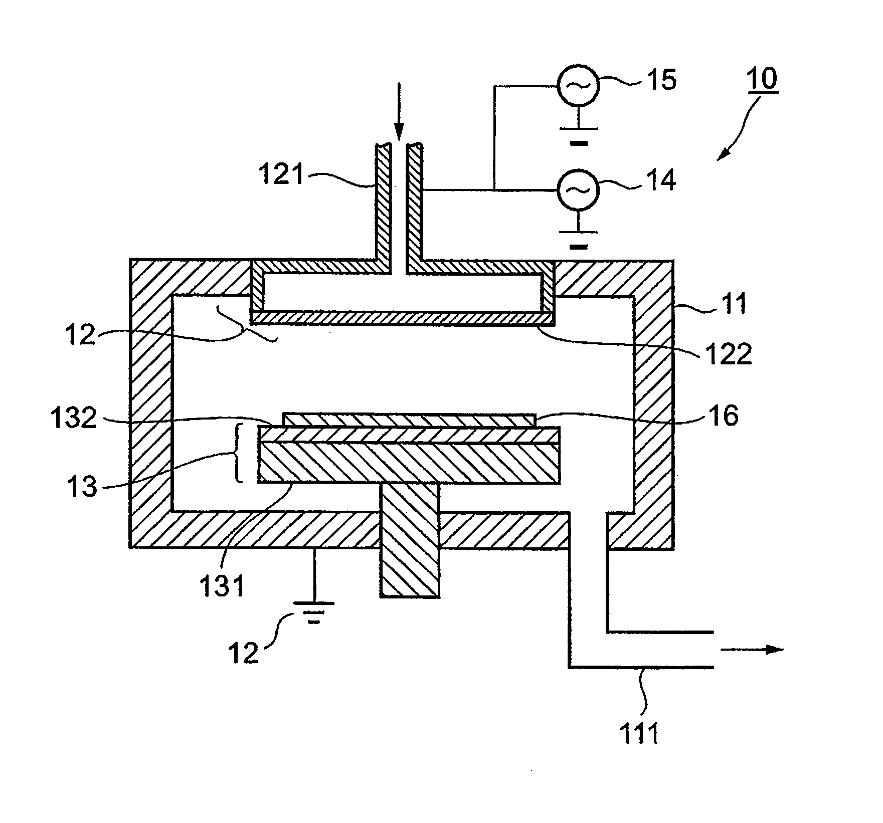
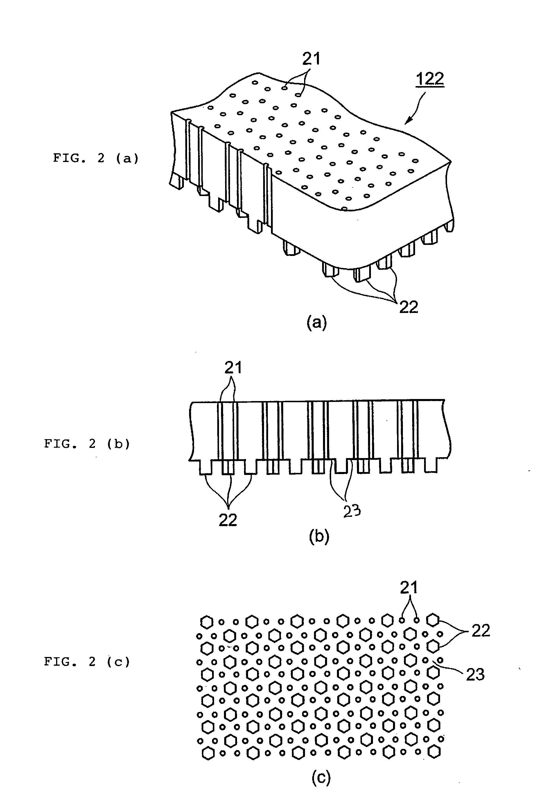
[0077] Thin film formation was conducted using the plasma CVD apparatus comprising the shower plate 22 shown in FIG. 2; and properties of thin films formed were measured (Examples 1-1 to 1-5). Additionally, as comparative examples, thin film formation was conducted using a plasma CVD apparatus comprising a shower plate similar to the shower plate described in U.S. Pat. No. 4,854,263; and properties of a thin film formed were measured. Specifications of the shower plates used are shown in Table 1 below. In Table 1, a rate of surface area increase is a rate of surface area increase as against a surface area of a tabular shower plate without protrusions or concave portions.
TABLE 1Example 1Comparative ExampleConfigurationHexagonalConcavecolumnHeight / depth3.7 mm3.8 mmWidth (face to face) / diameter 3 mm 3 mmPitch 6 mm4.2 mmThe number2,2334,005Increase of surface areaActual surface area89.8%152.8%0.5 mm sheath considered119.8%101.1%1.0 mm sheath considered149.7%50.6%
example 1-1
[0078] Film type: Low-deposition-rate silicon nitride film (Deposition rate<200 nm / min. (e.g., 160-190 nm / min.))
[0079] Deposition conditions:
[0080] Source gas 1: Silane (50-150 sccm, preferably 65-95 sccm)
[0081] Source gas 2: Ammonia (20-80 sccm, preferably 25-60 sccm)
[0082] Source gas 3: Nitrogen (5000-10000 sccm, preferably 7,500-10,000 sccm)
[0083] First RF power source (HRF): 13.56 MHz (1-1. 5 W / cm2—Anode reference)
[0084] Second RF power source (LRF): 400 kHz (0 W / cm2)
[0085] Pressure: 450-600 Pa (preferably 465-560 Pa)
[0086] Temperature: 300-400° C. (preferably 380-400° C.)
[0087] Workpiece: Diameter 300 mm silicon substrate
[0088] Cleaning frequency: Single wafer
[0089] Under the above-mentioned conditions, measurement results of properties of a thin film formed using the shower plate according to this embodiment of the present invention are shown in FIG. 4; measurement results of properties of a thin film formed using the shower head according to the related art are sho...
example 1-2
[0094] Film type: Low-deposition-rate silicon nitride thin film (Deposition rate<200 nm / min. (e.g., 160-190 nm / min.))
[0095] Deposition conditions:
[0096] Source gas 1: Silane (50-150 sccm, preferably 65-95 sccm)
[0097] Source gas 2: Ammonia (20-80 sccm, preferably 25-60 sccm)
[0098] Source gas 3: Nitrogen (5000-10000 sccm, preferably 7,500-10,000 sccm)
[0099] First RF power source (HRF): 13.56 MHz (0.72 W / cm2 fixed—Anode reference)
[0100] Second RF power source (LRF): 400 kHz (0.05-0.2 W / cm2—Anode reference)
[0101] Pressure: 450-600 Pa (preferably 465-560 Pa)
[0102] Temperature: 300-400° C. (preferably 380-400° C.)
[0103] Workpiece: Diameter 300 mm silicon substrate
[0104] Cleaning frequency: Single wafer
[0105] In this example, except that output of the first RF power source was fixed and that output of the second RF power source was changed, the same conditions as used for Example 1-1 were used. Under the above-mentioned conditions, measurement results of properties of a thin fil...
PUM
| Property | Measurement | Unit |
|---|---|---|
| Fraction | aaaaa | aaaaa |
| Width | aaaaa | aaaaa |
| Width | aaaaa | aaaaa |
Abstract
Description
Claims
Application Information