Semiconductor device and method of evaluating the same

a technology of semiconductor devices and integrated circuits, applied in semiconductor devices, semiconductor/solid-state device details, electrical devices, etc., can solve the problems of not obtaining impurity injection, reducing the hump characteristic, and not achieving the effect of simple shape of teg patterns, so as to reduce the number of man hours and costs, lessen the influence of curved portions, and reduce the effect of feedback from trial production

Active Publication Date: 2005-08-25
LAPIS SEMICON CO LTD
View PDF3 Cites 0 Cited by
  • Summary
  • Abstract
  • Description
  • Claims
  • Application Information

AI Technical Summary

Benefits of technology

[0023] According to the present invention as described above in detail, when an active region or a gate is bent approximately at right angles, the interval between patterns for the active region and the gate is set larger than an arc radius of a substantially arcuate curved portion lying inside the pattern for

Problems solved by technology

On the other hand, however, each of patterns for an active region and a gate in an actual circuit pattern cannot be configured in a simple shape like a TEG pattern.
When a curved active region overlaps a gate pattern even in the case of the i

Method used


Image

  • Semiconductor device and method of evaluating the same
  • Semiconductor device and method of evaluating the same
  • Semiconductor device and method of evaluating the same

Examples


Embodiment Construction

[0032] Preferred embodiments of the present invention will be explained hereinafter in detail with reference to the accompanying drawings. Incidentally, elements each having substantially the same functional constitution are given like reference numerals through this specification and figures, and dual explanations of the same elements will therefore be avoided.

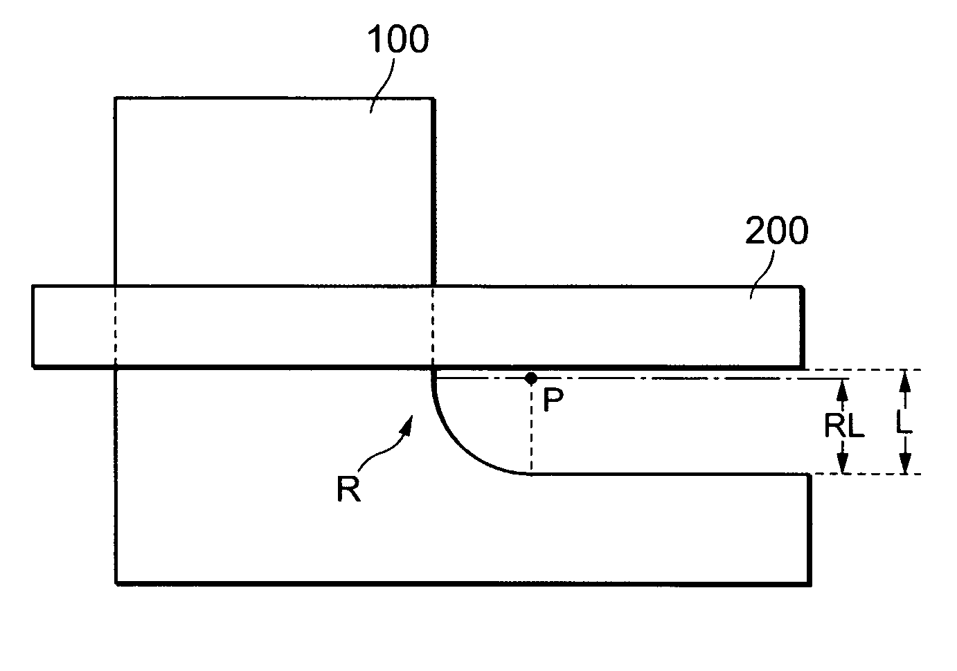
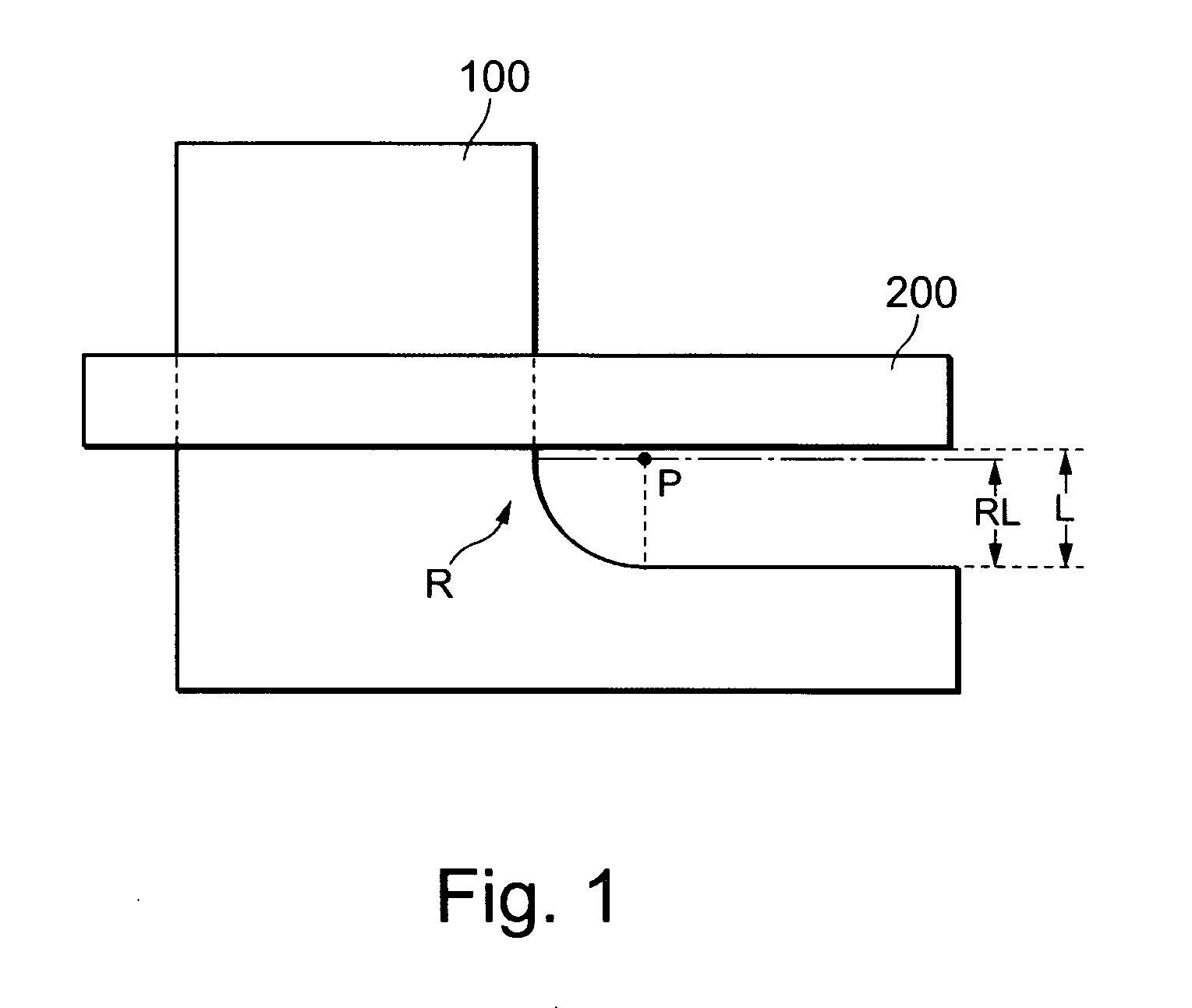
[0033] A description will be made of a case in which an active region 100 of a MOS transistor such as shown in FIG. 1 as the present embodiment is bent at right angles. The present embodiment is characterized in that an interval L between the active region 100 and a gate 200 is made larger than an arc radius RL at an arcuate curved portion R of the active region. Here, the term “at right angles” does not mean an accurate angle of 90° but a pattern bent substantially at right angles. Also the term “arcuate” does not mean a line that accurately overlaps the arc of a circle but means that the line can be handled as a circular a...


PUM


Abstract

The present invention provides a semiconductor device having an active region bent at right angles, wherein an interval between patterns for the active region and a gate is set larger than an arc radius of a curved portion (portion where a line is brought to arcuate form) formed inside the pattern for the bent active region. By defining and designing the pattern interval, the curved portion of the active region do not overlap the gate pattern, and the difference between a device characteristic and a designed value can be prevented from increasing.

Description

BACKGROUND OF THE INVENTION [0001] 1. Field of the Invention [0002] The present invention relates to a transistor integrated circuit formed on a wafer, and particularly to a semiconductor device capable of obtaining a characteristic equivalent to a design value where an active region or a gate of a MOS transistor is a bent pattern, and a method of evaluating the semiconductor device. [0003] 2. Description of the Related Art [0004] With the objective of speeding up a device, an SOI (Silicon On Insulator) substrate in which a thin silicon layer is formed on an insulating layer, has been in heavy usage in recent years. A method of forming a transistor on an SOI is basically similar to a process using a bulk silicon wafer. [0005] When device isolation is carried out by a LOCOS (Local Oxidation Of Silicon) method at this time, the edges of an SOI layer provided on a buried oxide film 2 are brought to bird beaks due to a LOCOS oxide film 1 as shown in FIG. 4A. When a gate oxide film 4 is ...

Claims


Application Information

Patent Timeline
IPC IPC(8): H01L29/06H01L29/76H01L29/786
CPCH01L29/0657H01L29/78696H01L29/78654H01L29/78606
Inventor KISHIRO, KOICHI
Owner LAPIS SEMICON CO LTD
Why Eureka
Try Eureka