Semiconductor package free of substrate and fabrication method thereof
- Summary
- Abstract
- Description
- Claims
- Application Information
AI Technical Summary
Benefits of technology
Problems solved by technology
Method used
Image
Examples
second preferred embodiment
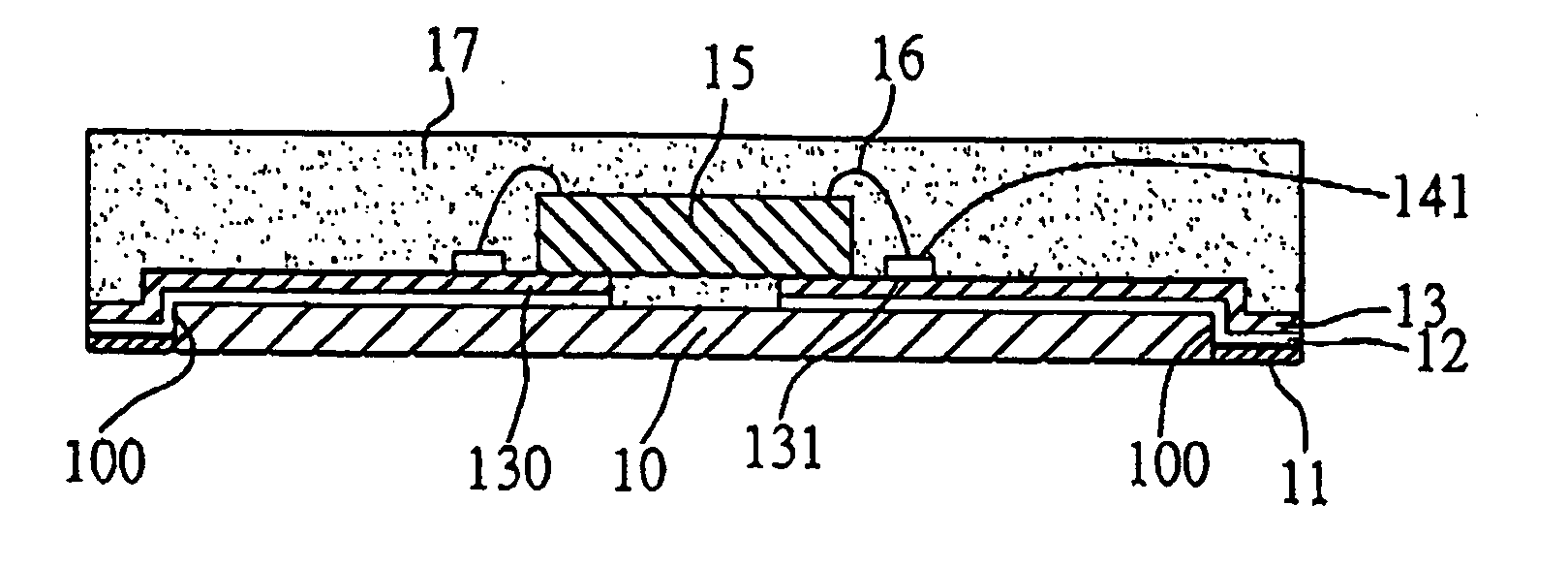
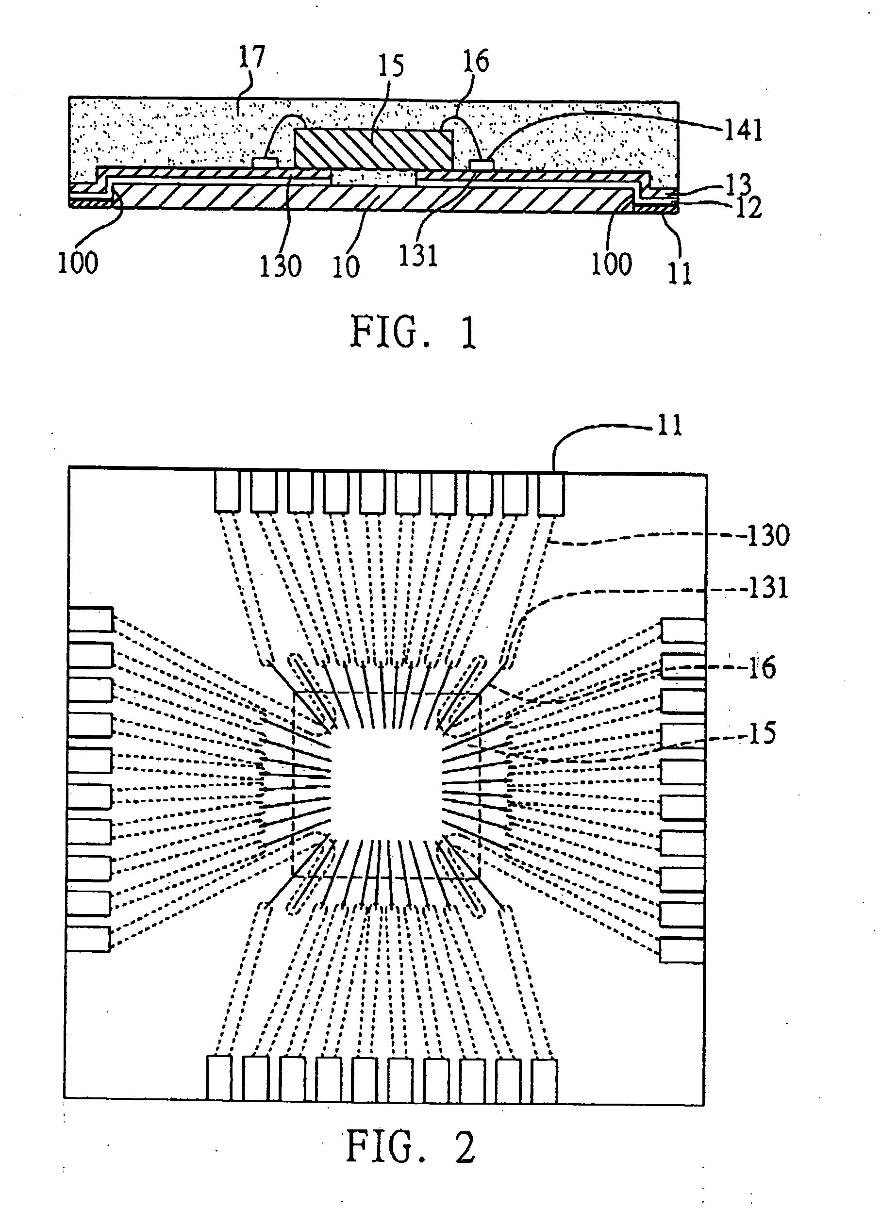
[0046]FIG. 4 illustrates a semiconductor package according to a second preferred embodiment of the invention. As shown in the drawing, this semiconductor package differs from that of the above first embodiment in that the chip 15 is mounted in a flip-chip manner on the conductive traces 130. In particular, during a die bonding process, the active surface 150 of the chip 15 is directed toward the conductive traces 130 and electrically connected via solder bumps 16′ to the terminals 131 of the conductive traces 130 where the terminals 131 serve as bond pads used to be bonded with the solder bumps 16′. Alternatively, an insulating layer 140 can be applied over the conductive traces 130 with the terminals 131 being exposed and connected to the solder bumps 16′.
[0047] Compared to the use of bonding wires for electrically connecting the chip and conductive traces, the flip-chip technology can further reduce an electrical connection distance from the chip 15 to conductive traces 130 via s...
third preferred embodiment
[0049]FIG. 5 illustrates a semiconductor package according to a third preferred embodiment of the invention. This semiconductor package differs from that of the above first embodiment in that a plurality of solder balls 19 are implanted on the exposed solder materials 11 to form a ball grid array. These solder balls 19 serve as I / O connections of the semiconductor package to be electrically connected with an external device (not shown).
fourth preferred embodiment
[0050]FIG. 10 shows a carrier structure for semiconductor package according to a fourth preferred embodiment of the invention. As shown in FIG. 10, this carrier structure comprises a dielectric material layer 10 formed with a plurality of openings 100 penetrating the same; a conductive material 11 applied in the openings 100 of the dielectric material layer 10; and a conductive layer 1 formed on the dielectric material layer 10 and the conductive material 11, wherein the conductive layer 1 comprises a plurality of conductive traces 130, and each of the conductive traces 130 has a terminal 131.
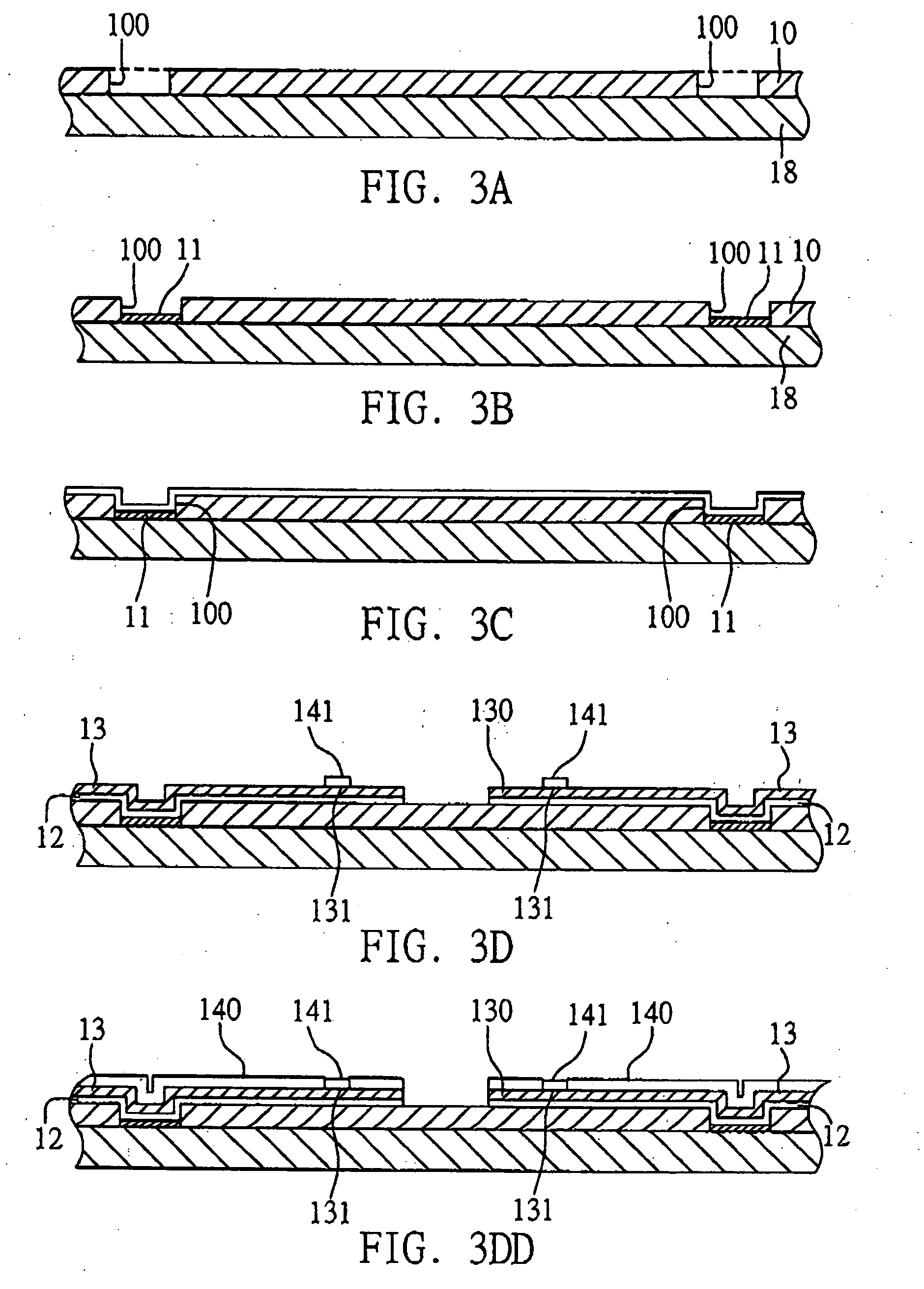
[0051] In the fabrication method of the carrier structure shown in FIG. 10, after the processes shown in FIGS. 3A and 3B that a metal carrier 18 is prepared and applied with a dielectric material layer 10 thereon having a plurality of openings 100, and a conductive material such as a solder material 11 is deposited in the openings 100 of the dielectric material layer 10, referring to FIG. 11A,...
PUM
 Abstract
Description
Claims
Application Information


