Electron emission device and method of manufacturing the same

Inactive Publication Date: 2005-08-25
SAMSUNG SDI CO LTD
View PDF3 Cites 6 Cited by
  • Summary
  • Abstract
  • Description
  • Claims
  • Application Information

AI Technical Summary

Benefits of technology

[0013] It is yet another object of the present invention to provide an electron emission device and a method of manufactu

Problems solved by technology

When ultraviolet rays are illuminate the electron emission material from the front side of the first substrate during the light-exposing step, the pattern of the electron emission regions is non-uniformly made, and the adhesion of the electron emission regions to the cathode electrodes is poor.
However, a structure pr

Method used


Image

  • Electron emission device and method of manufacturing the same
  • Electron emission device and method of manufacturing the same
  • Electron emission device and method of manufacturing the same

Examples


Example

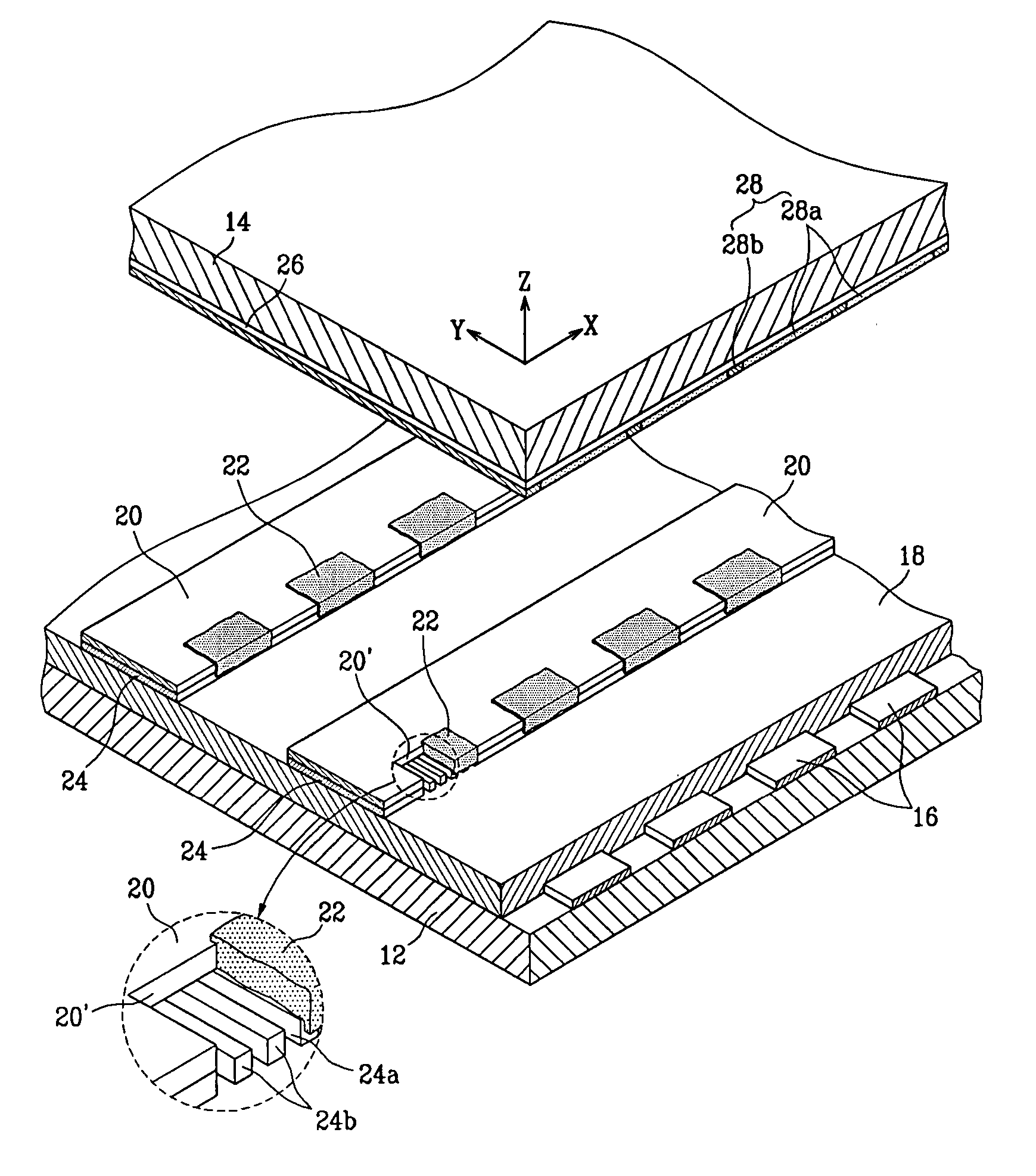
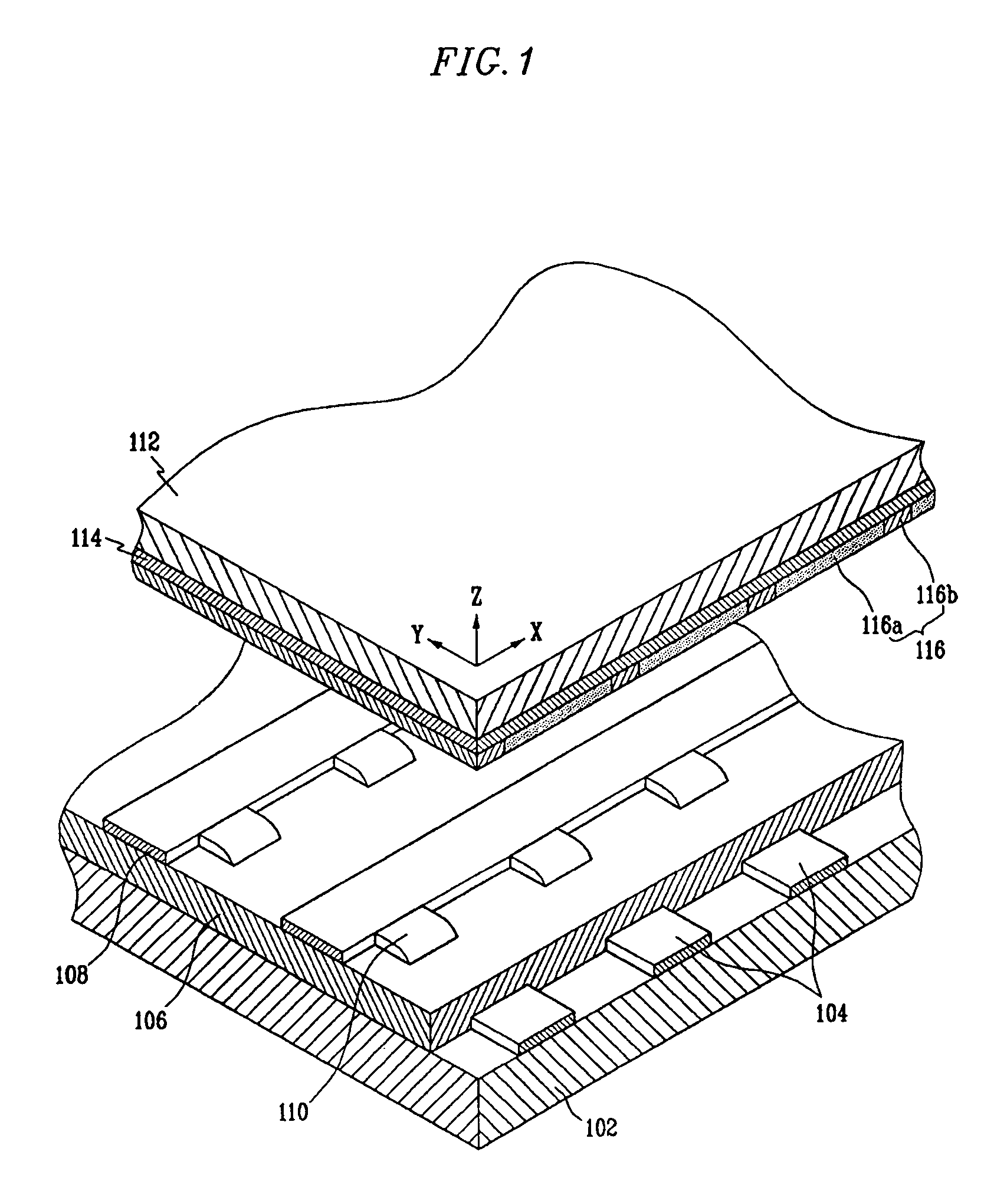
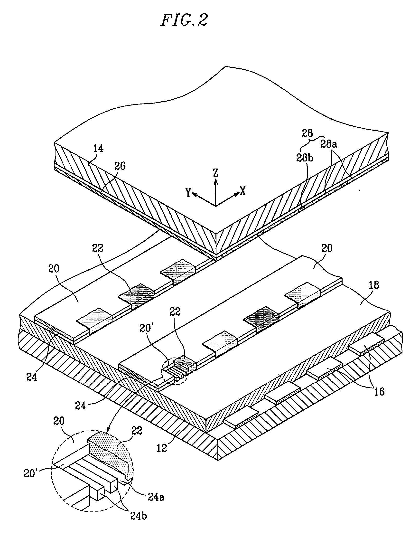
[0026] An electron emission device where the electron emission regions are made using the backside exposure technique is illustrated in FIG. 1. As illustrated in FIG. 1, transparent gate electrodes 104 are formed on a first transparent substrate 102. An insulating layer 106 is formed on the entire inner surface of the first substrate 102 using a transparent material such that it covers the gate electrodes 104. Cathode electrodes 108 are formed on the insulating layer 106 by coating a metallic material, such as chromium Cr, thereon, and patterning it.

[0027] Electron emission regions 110 are formed at the lateral side of the respective cathode electrodes 108 by coating a carbonaceous and / or nano-sized electron emission material on the insulating layer 106, and exposing it to light using the backside exposure technique. Specifically, the formation of the electron emission regions 110 is made by first forming a sacrificial layer (not illustrated) on the cathode electrodes 108 and on th...


PUM


Abstract

A structure for a field emission device and a method of making the same. The cathode electrodes are formed as a two-layered structure of chromium on top of aluminum. Photosensitive electron emission material is patterned via back side exposing, the aluminum layer serving as a mask. In receptor regions, conducting aluminum fingers form electrical contact with the emission material while spaces between the aluminum fingers serve as a window to allow for exposure of the photosensitive emission material.

Description

CLAIM OF PRIORITY [0001] This application makes reference to, incorporates the same herein, and claims all benefits accruing under 35 U.S.C. § 119 from an application for FIELD EMISSION DISPLAY DEVICE AND MANUFACTURING METHOD OF THE SAME earlier filed in the Korean Intellectual Property Office on 20 Feb. 2004 and there duly assigned Ser. No. 10-2004-0011391. BACKGROUND OF THE INVENTION [0002] 1. Technical Field [0003] The present invention relates to an electron emission device, and in particular, to an electron emission region and a method of manufacturing the same. [0004] 2. Description of the Related Art [0005] Generally, the electron emission devices are classified into a first type where a hot cathode is used as an electron emission source, and a second type where a cold cathode is used as the electron emission source. The second type of electron emission devices include a field emitter array (FEA) type, a surface conduction emitter (SCE) type, a metal-insulator-metal (MIM) typ...

Claims


Application Information

Patent Timeline
IPC IPC(8): H01J1/304H01J1/62H01J3/02H01J9/02H01J63/04
CPCH01J9/025H01J3/022H01J1/304H01J2201/30446H01J2201/30469
Inventor RYU, KYUNG-SUN
Owner SAMSUNG SDI CO LTD
Why Eureka
Try Eureka