Implementing low power level shifter for high performance integrated circuits

a technology of integrated circuits and shifters, applied in the field of data processing, can solve the problems of limiting the performance of the circuit, reducing the power and performance characteristics of the level shifter circuit b>300/b>, and so as to increase the functionality of the level shifter and improve the power and performance characteristics. the effect of reducing the overall delay

Inactive Publication Date: 2009-07-09
IBM CORP
View PDF8 Cites 1 Cited by
  • Summary
  • Abstract
  • Description
  • Claims
  • Application Information

AI Technical Summary

Benefits of technology

[0014]In accordance with features of the invention, the level shifter circuit enables enhanced power and performance characteristics. The level shifter circuits reduce overall delay, increase level shifting functionality, and enable more flexibility in device sizing for circuit performance.

Problems solved by technology

As shown in FIGS. 1A, and 1B when static logic gates are connected normally at the interface between a lower VDDA and a higher VDDB, problems can result.
Problems with many known level shifter circuits include degraded power and performance characteristics.
Also prior art level shifter circuit 300 fails to enable high frequency operation that may be required for some particular applications.
A disadvantage to the low power level shifter circuit shown in FIG. 4 is that it is very sensitive to the ratio of device strengths PFET 416 and NFET 404.
This constraint can limit the performance of the circuit.

Method used


Image

  • Implementing low power level shifter for high performance integrated circuits
  • Implementing low power level shifter for high performance integrated circuits
  • Implementing low power level shifter for high performance integrated circuits

Examples


Embodiment Construction

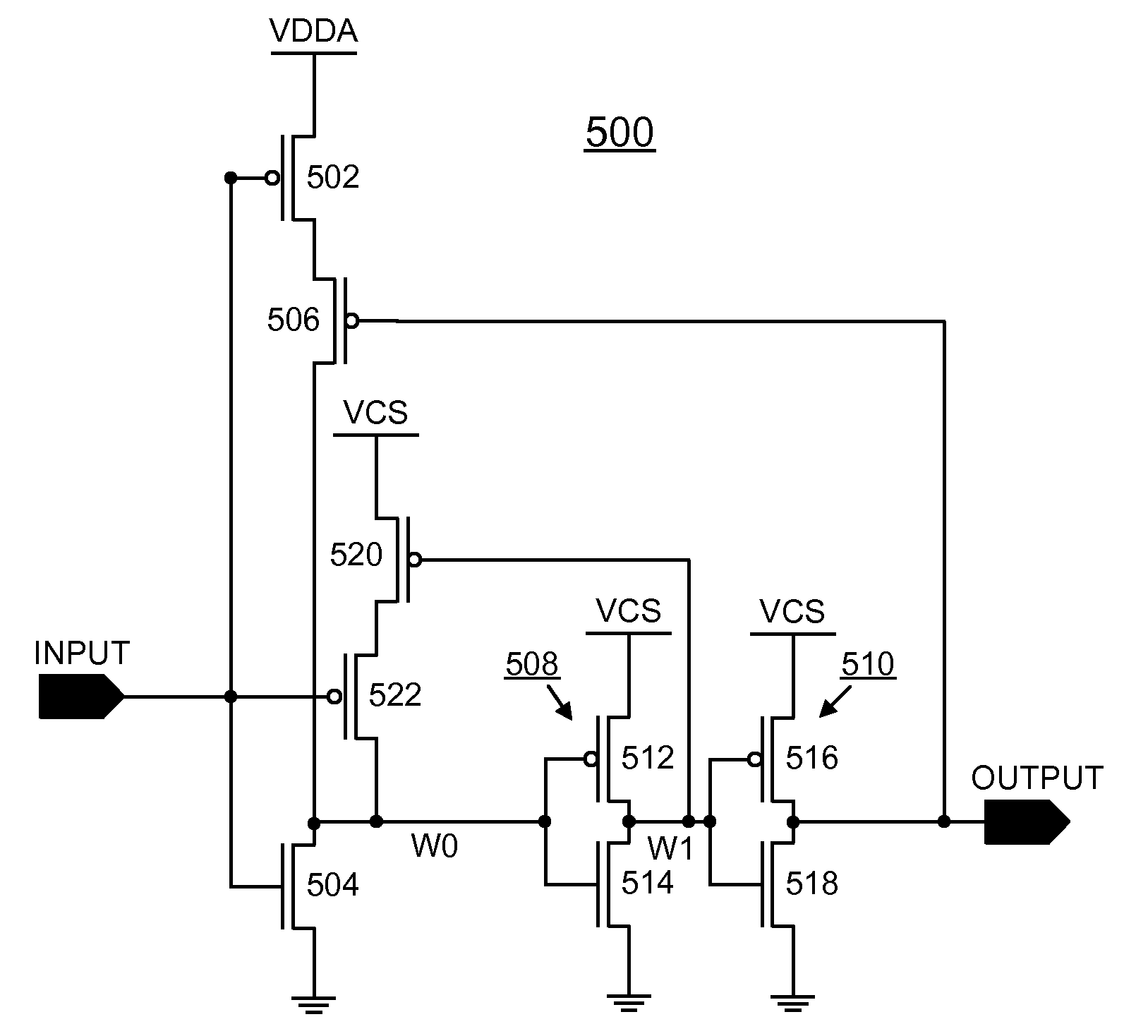
[0022]In accordance with features of the invention, level shifter circuits are provided having excellent power and performance characteristics, providing improved performance characteristics over known level shifter circuits, such as shown in FIG. 4. The novel level shifter circuits reduce overall delay, increase level shifting functionality, have slightly better input noise immunity for “rising above ground” noise, and enable more flexibility in device sizing for circuit performance. This method for implementing the level shifter circuits advantageously is applied to various static logic circuits.

[0023]Having reference now to the drawings, in FIG. 5, there is shown an exemplary level shifter circuit generally designated by the reference character 500 in accordance with the preferred embodiment. Level shifter circuit 500 includes an input stage P-channel field effect transistor (PFET) 502 and an N-channel field effect transistor (NFET) 504 receiving an input signal INPUT. PFET 502 i...


PUM


Abstract

A low power level shifter circuit for high performance integrated circuits includes an input inverter operating in a domain of a first voltage supply and receiving an input signal and a design structure on which the subject circuit resides is provided. An output stage operating in a domain of a higher second voltage supply includes a first output inverter connected to the input inverter and a second output inverter connected in series with the first output inverter. The second output inverter provides a level shifted output signal having a voltage level corresponding to the second voltage supply. A series connected finisher transistor and finisher control transistor are connected between the second voltage supply and an input to the first output inverter. The finisher control transistor is activated responsive to the input signal. A path control transistor controls a path between the first voltage supply and the input inverter. The path control transistor being activated responsive to the level shifted output signal.

Description

FIELD OF THE INVENTION[0001]The present invention relates generally to the data processing field, and more particularly, relates to a low power level shifter circuit and a method for implementing low power level shifter circuits for high performance integrated circuits, and a design structure on which the subject circuit resides.DESCRIPTION OF THE RELATED ART[0002]As technology advances, scaling of the power supply voltage occurs for power reduction and reliability reasons. Certain types of circuits are more sensitive to this reduction in voltage such as analog, memory and input / output (I / O) circuits. To combat this, many chip designs have added extra power supply domains to use in these sensitive circuits.[0003]Level shifter circuits are utilized in integrated circuits for changing the voltage of a signal from a first voltage to a second voltage, such as from a high to a low operating voltage, or from a low to a high operating voltage.[0004]Referring to FIGS. 1A, and 1B, there is s...

Claims


Application Information

Patent Timeline
Patent Type & Authority Applications(United States)
IPC IPC(8): H03L5/00
CPCH03K3/356165H03K3/012
Inventor BEHRENDS, DERICK GARDNERCHRISTENSEN, TODD ALANHEBIG, TRAVIS REYNOLD
Owner IBM CORP
Why Eureka
Try Eureka