Flexible printed circuit board

Inactive Publication Date: 2005-09-01
ALPS ALPINE CO LTD
View PDF3 Cites 15 Cited by
  • Summary
  • Abstract
  • Description
  • Claims
  • Application Information

AI Technical Summary

Benefits of technology

[0012] In view of the problems described above, it is an object of the present invention to provide an FPC board including a built-in antistatic circuit. The FPC board does not cause electrostatic damage to an optical pickup element, a preamplifier element, and a magnetic head including a micro circuit, thereby improving the yield. The FPC board also eliminates limitations on the packaging of an optical pickup element, a preamplifier element, a magnetic head, and the like.
[0018] The FPC board according to the present invention includes the electrostatic protection circuit built in the substrate layer, on which the wiring layers are disposed. The built-in electrostatic protection circuit is composed of the thin-film capacitor element including a thin-film dielectric layer sandwiched between thin-film conductive layers. Since this FPC board does not need an additional antistatic chip such as a CR element chip, the following advantages can be achieved. The FPC board ensures its flexibility because the FPC board does not include a portion carrying the additional antistatic chip. No additional step for mounting the additional antistatic chip is required, whereas a known FPC board requires an additional step for mounting the antistatic chip preceding a step for mounting, for example, a magnetic head and an optical pickup. No additional space for mounting the additional antistatic chip is required, and a small FPC can be achieved. Moreover, since the electrostatic protection circuit is built in the FPC board in advance, static electricity is less likely to cause electrostatic damage to, for example, a hard disk drive including a magnetic head and a device including an optical pickup in the assembly operation.
[0019] In the FPC board according to the present invention, the terminals are disposed under the resin mold segment of the element chip to be mounted on the FPC board to connect to the connectors of the element chip. Since the wiring circuit is entirely covered with the element chip, there is no exposed portion that functions as an antenna erroneously receiving noise as signals. Moreover, since the wiring path between the element chip and the electrostatic protection circuit can be shortened, parasitic inductance can be reduced, thereby maximizing the antistatic effects of the thin-film capacitor element on the discharge of static electricity having a high-frequency component of one gigahertz or more.

Problems solved by technology

Thus, static electricity easily causes damage to the magnetic head.
For example, static electricity is built up in a hard disk drive when a worker touches the hard disk drive in the assembly operation, and the static electricity may cause damage to the GMR element or cause malfunction of the GMR element when the hard disk drive is used.
Thus, malfunction and damage are easily caused by static electricity.
In the assembly operation, before electric charge having a polarity opposite to that of the electric charge of the built-up static electricity is supplied to the FPC board to prevent the static electricity, the static electricity may have an adverse effect on a micro-magnetic circuit in a magnetic head and may have an adverse effect, for example, malfunction, on various elements, for example, a preamplifier provided at some point in a circuit, an optical pickup, and a laser chip.
When a dedicated chip serving as a protection circuit is additionally installed, the following problems occur.
Also, in the FPC board, flexibility of a portion carrying the chip serving as a protection circuit is impaired.
Although the FPC board needs to quickly move along with a magnetic head moving at high speed, such a magnetic head loses its balance when the FPC board is less flexible.
Moreover, in the FPC board, additional space is required for mounting the CR chip in addition to the required elements, for example, the magnetic head and a laser chip.

Method used


Image

  • Flexible printed circuit board
  • Flexible printed circuit board
  • Flexible printed circuit board

Examples


example

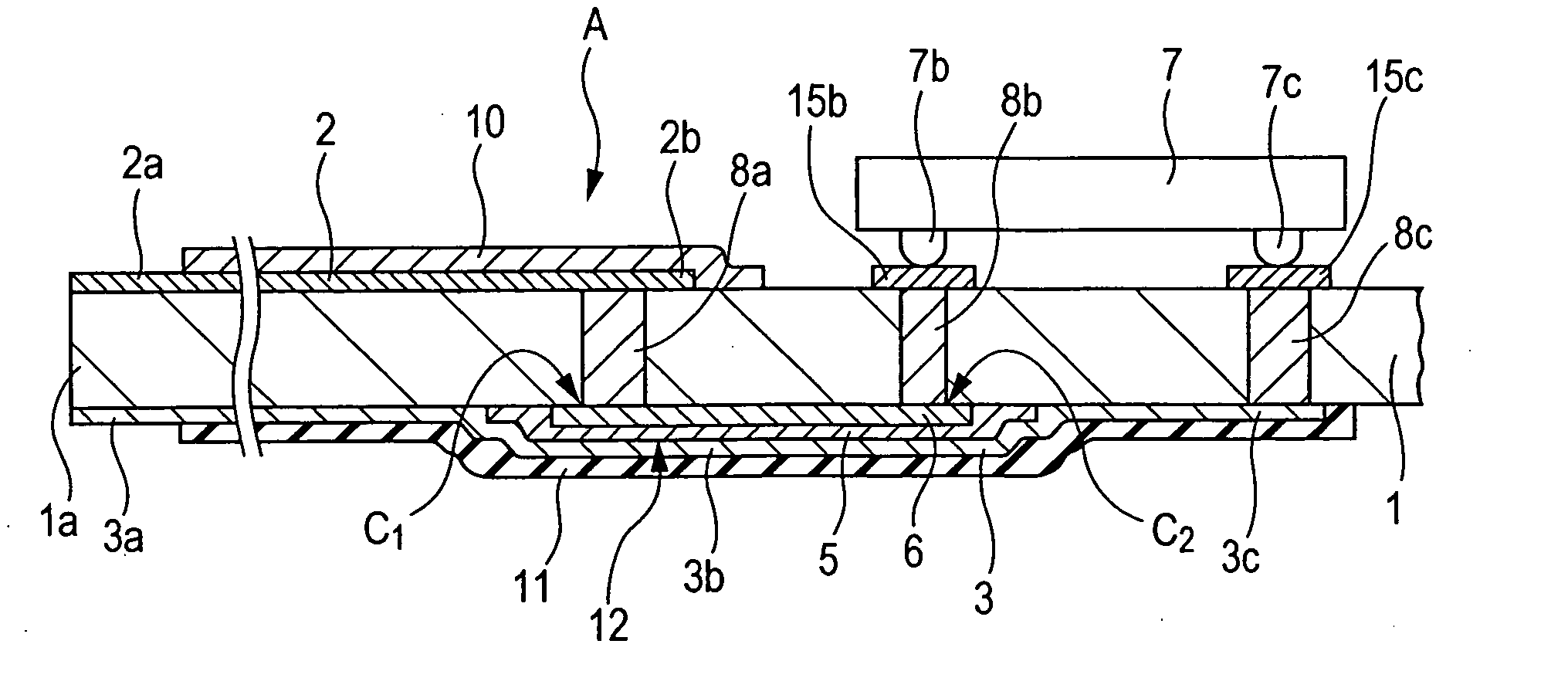
[0051] Under the condition that a laser diode (LD) element serving as an optical pickup device is used in place of the element chip 7 in the circuit shown in FIG. 2, electrostatic breakdown voltages of the LD element were examined at several capacitances, including zero, of thin-film capacitor elements. Examination was carried out using the charged device model (CDM). The resistance R was 35 Ω. A red laser diode mainly composed of a GaAs substrate was used as the LD element. Table I shows the results of the examination.

TABLE ICapacitance of Capacitors C1 Breakdown Voltageand C2 (unit: μF)(unit: KV)1.01.40.51.40.11.40.021.40.011.400.5

[0052] Apparently, the results indicated in Table I show that the electrostatic breakdown voltages of the optical pickup device were improved when the capacitors C1 and C2 were charged. While the first wiring layer 22 and the second wiring layer 23, which generally have a thickness of about 25 μm in the second embodiment, ensure flexibility of the FPC ...


PUM


Abstract

A flexible printed circuit board includes a substrate layer composed of insulating material, a protection circuit of a thin-film capacitor element, the protection circuit including a first wiring layer on the substrate layer, a dielectric layer, and a counter electrode layer. At least a portion of each of the first wiring layer and the counter electrode layer serves as a terminal. The front surface of each of the first wiring layer and the counter electrode layer, except the terminal portion, is covered with an insulating coating.

Description

BACKGROUND OF THE INVENTION [0001] 1. Field of the Invention [0002] The present invention relates to antistatic flexible printed circuit (FPC) boards that do not cause electrostatic damage to electrical components connected to the FPC boards. [0003] 2. Description of the Related Art [0004] Hard disk drives are often used in, for example, magnetic recording devices for computers and video recording / playback devices. A hard disk drive includes a rotatable disk including a magnetic recording layer. In a hard disk drive, a magnetic head attached to a tip of a metallic leaf spring called a load beam moves relative to the disk surface to write and read data magnetically. [0005] The magnetic head, including a micro-magnetic circuit, for example, a giant magnetoresistive (GMR) element, is mounted on a moving ceramic part called a slider. While the leaf spring urges the bottom surface of the slider toward the disk surface, wind pressure caused by the spinning of the disk is applied to the sl...

Claims


Application Information

Patent Timeline
IPC IPC(8): G02F1/1345H05K1/02H05K1/11H05K1/16H05K1/18H05K3/28H05K9/00
CPCH05K1/113H05K1/162H05K1/189H05K3/28H01L2224/16H05K2201/09763H05K2201/09772H05K2201/10674H05K2201/0317G11B5/40G11B5/486
Inventor NAKANO, AKIRATSUJI, YOSHIOMIHIGA, YOSHINARI
Owner ALPS ALPINE CO LTD
Why Eureka
Try Eureka