Method of observing a specimen using a scanning electron microscope

Active Publication Date: 2005-09-08
HITACHI HIGH-TECH CORP
View PDF3 Cites 16 Cited by
  • Summary
  • Abstract
  • Description
  • Claims
  • Application Information

AI Technical Summary

Benefits of technology

[0014] It is an object of the present invention to provide a method of observing a specimen, using a scanning electron microscope, to make it possible the time necessary for automatic

Problems solved by technology

On the other hand, the wide-field (low resolution) image might oft

Method used


Image

  • Method of observing a specimen using a scanning electron microscope
  • Method of observing a specimen using a scanning electron microscope
  • Method of observing a specimen using a scanning electron microscope

Examples


Example

[0031] The present invention will be described hereafter in detail with reference to the accompanying drawings.

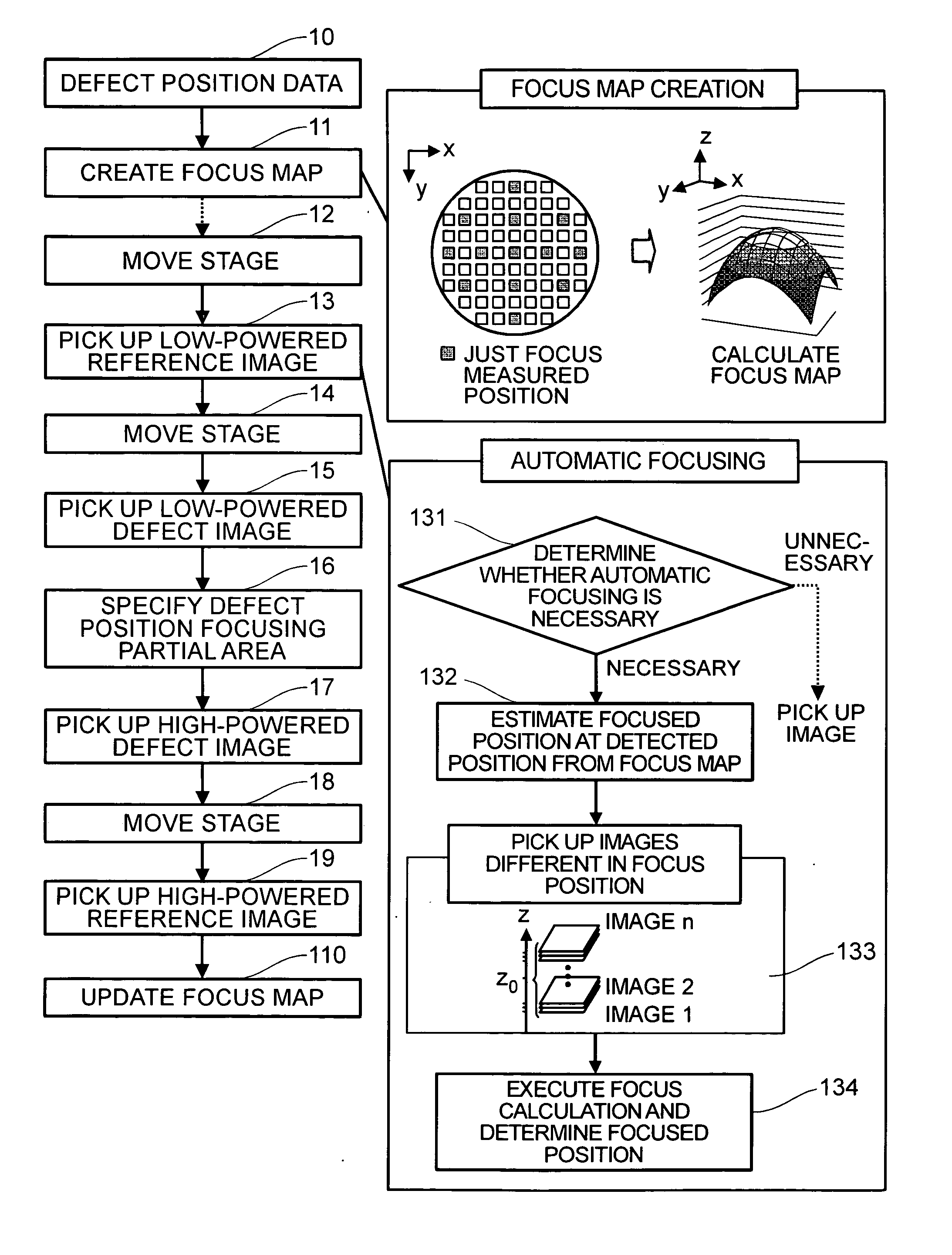
[0032]FIG. 1 shows an image pickup sequence for use in carrying out an automatic defect review according to the present invention.

[0033] In FIG. 1, reference numeral 10 indicates defect position data. Prior to the review, coordinate positions on a wafer, where respective defects have been detected by an optical or electron beam inspecting device, are inputted to a review electron beam microscope as the defect position data 10.

[0034] Next, a focus map creating process 11 is performed prior to the picking-up of images of the respective defects. Focus positions are determined or measured at a plurality of points (about several to ten points or more, which are not necessarily limited to defects) by manual control, and a curved surface sufficient to produce a good approximation of the result of measurement of the focus positions is estimated. This can be mathematically formul...


PUM


Abstract

A method of observing a specimen using a scanning electron microscope, makes it possible to shorten the time required to perform automatic focusing at the time of semiconductor defect automatic review and improves the throughput in the processing in which the specimen is observed. In the above method, the specimen is imaged at a low resolution by the scanning electron microscope to obtain an image, an area for imaging the specimen at a high resolution is specified from the image acquired at the low resolution, the specimen is imaged at a high resolution by the scanning electron microscope to determine a focus position, a focal point of the scanning electron microscope is set to the determined focus position, and a high resolution image in the specified area is acquired in a state in which the focus position has been set to the determined focus position.

Description

BACKGROUND OF THE INVENTION [0001] The present invention relates to a method of observing a specimen using a scanning electron microscope for reviewing defects on the surfaces of a semiconductor electronic circuit substrate, a liquid crystal display substrate, etc. [0002] With the objective of determining in detail each defect produced on a semiconductor electronic circuit substrate, automatic defect review (ADR: Automatic Defect Review) has been carried out for re-detecting an image at each defect position, detected by an optical inspecting device or an electron beam inspecting device, with high resolution by use of an electron beam microscope. The automatic defect review involves the collection of images of a large number of defects that are identified by the inspecting device automatically and at high speed. [0003] As an example of such automatic defect review, reference is made, for example, to Japanese Patent Laid-open No. 2002-124555 and Japanese Patent Laid-open No. 2003-9811...

Claims


Application Information

Patent Timeline
IPC IPC(8): G21K7/00
CPCH01J37/21H01J2237/2817H01J2237/216H01J37/28
Inventor OKUDA, HIROHITOHONDA, TOSHIFUMIAOKI, KAZUOYAMAGUCHI, KOHEISAKAMOTO, MASASHI
Owner HITACHI HIGH-TECH CORP
Why Eureka
Try Eureka