Semiconductor package free of substrate and fabrication method thereof

a technology of semiconductors and substrates, applied in the direction of semiconductor devices, semiconductor/solid-state device details, electrical apparatus, etc., can solve the problems of easy wire sweep or shift, short circuit, and difficult implementation of wire bonding process, so as to reduce the electrical connection path, shorten the bonding wire used, and eliminate the difficulty in performing the wire bonding process

Inactive Publication Date: 2005-09-08
HUANG CHIEN PING +2
View PDF19 Cites 8 Cited by
  • Summary
  • Abstract
  • Description
  • Claims
  • Application Information

AI Technical Summary

Benefits of technology

[0018] The semiconductor package in the present invention yields a significant benefit as not having to use a substrate or lead frame as a chip carrier; instead, a chip is mounted on conductive traces which can be flexibly arranged according to bond pad distribution of the chip. The flexible arrangement of conductive traces can effectively shorten the bonding wires used for electrically connecting the chip to terminals (bond fingers) of the conductive traces, thereby reducing an electrical connection path between the chip and conductive traces. As a result, the prior-art problems such as short circuits caused by long bonding wires and difficulty in performing the wire bonding process can be eliminated. Moreover, fabrication costs for the semiconductor package are also desirably reduced without having to use a substrate or lead frame.

Problems solved by technology

Long bonding wires 22′, however, make a wire bonding process harder to implement and are easily subject to wire sweep or shift due to resin flow impact in a molding process for forming the encapsulant 23.
The swept or shifted bonding wires may accidentally come into contact with each other and cause short circuits, which would undesirably degrade quality of electrical connection.
Further, if the leads and die pad are spaced apart from each other too far, the wire bonding process may even be impossibly performed and thus fails to use bonding wires to electrically connect the chip to the leads of the lead frame.
However, fabrication of the protruding portions 213 would undesirably increase costs and process complexity for making the lead frame 21′.
However, similarly to the previously discussed packaging technology, in the case of using a highly integrated chip 33 with more bond pads or higher density of bond pads, more contacts 32 are accordingly required and undesirably increase the distance between the contacts 32 and chip 33, thereby causing the similar problems as shown in FIG. 7B that long bonding wires are subject to wire sweep or shift and degrade quality of electrical connection.

Method used


Image

  • Semiconductor package free of substrate and fabrication method thereof
  • Semiconductor package free of substrate and fabrication method thereof
  • Semiconductor package free of substrate and fabrication method thereof

Examples


first preferred embodiment

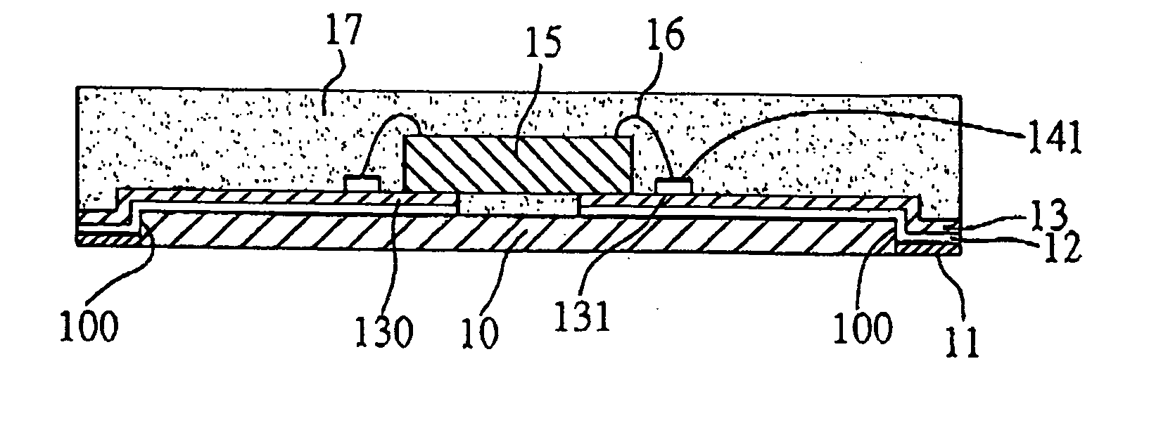
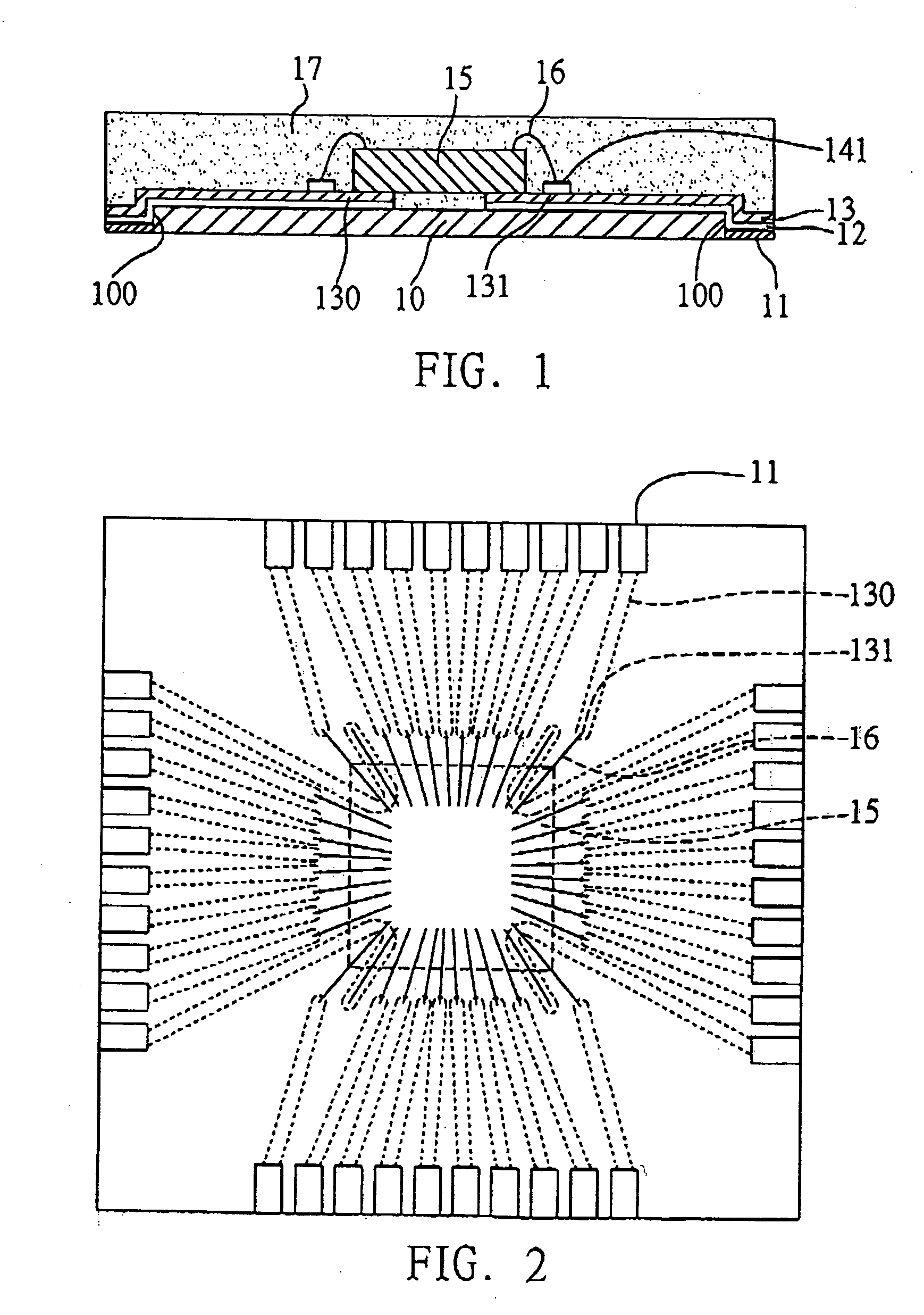
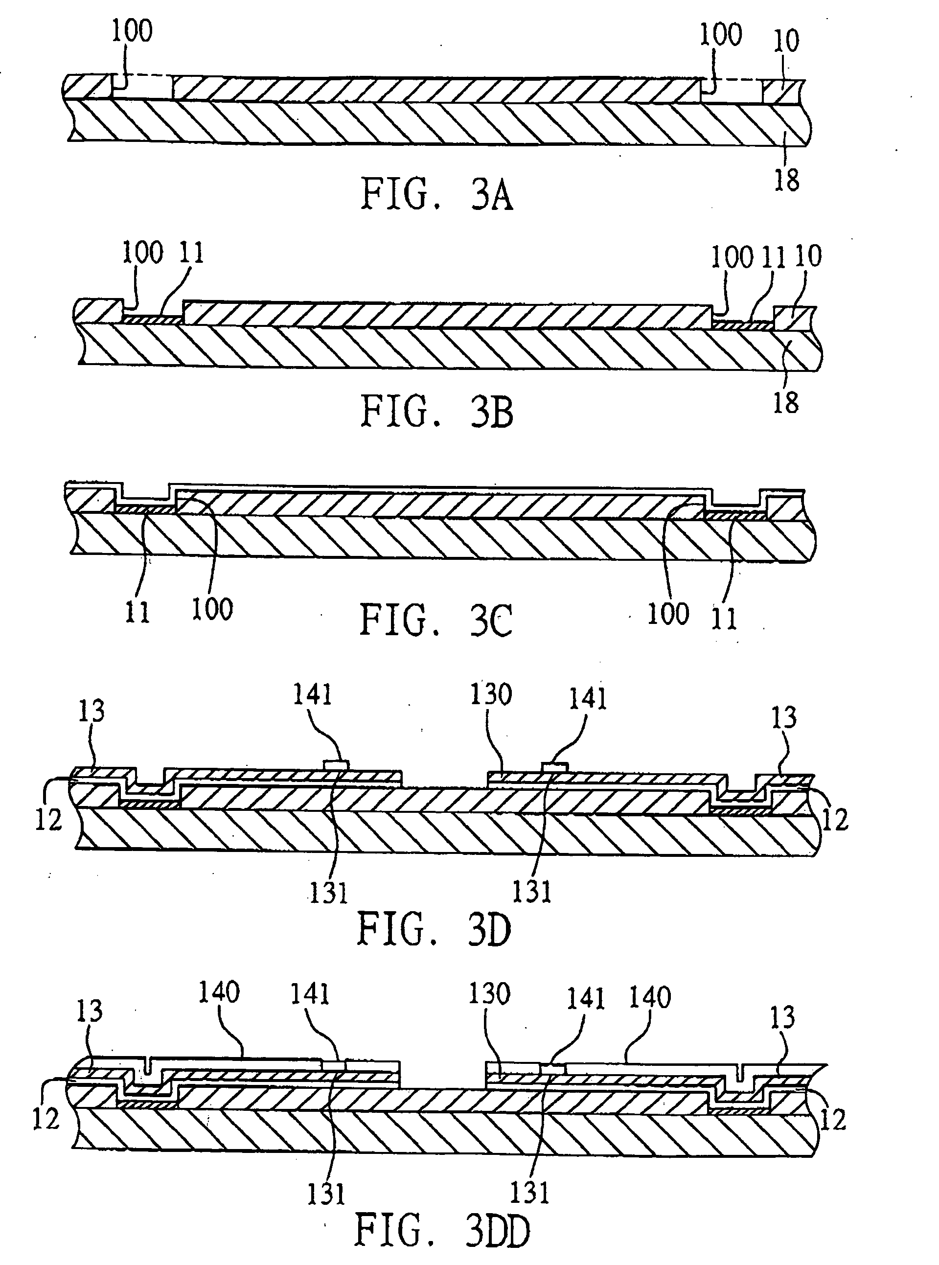
[0032] The present invention provides a semiconductor package free of using a substrate; as shown in FIGS. 1 and 2, this semiconductor package includes a dielectric material layer 10 formed with a plurality of openings 100 penetrating through the dielectric material layer 10; a solder material 111 applied in each of the openings 100; a first copper layer 12 formed over the dielectric material layer 10 and solder materials 11 in the openings 100; a second copper layer 13 formed over the first copper layer 12, allowing the first and second copper layers 12, 13 to be patterned to form a plurality of conductive traces 130 each having a terminal 131, wherein the first copper layer 12 is smaller in thickness than the second copper layer 13; a metal layer 141 applied on each of the terminals 131; at least one chip 15 mounted on a predetermined portion of the conductive traces 130; a plurality of bonding wires 16 for electrically connecting the chip 15 to the metal layers 141 of the termina...

second preferred embodiment

[0045]FIG. 4 illustrates a semiconductor package according to a second preferred embodiment of the invention. As shown in the drawing, this semiconductor package differs from that of the above first embodiment in that the chip 15 is mounted in a flip-chip manner on the conductive traces 130. In particular, during a die bonding process, the active surface 150 of the chip 15 is directed toward the conductive traces 130 and electrically connected via solder bumps 16′ to the terminals 131 of the conductive traces 130 where the terminals 131 serve as bond pads used to be bonded with the solder bumps 16′. Alternatively, an insulating layer 140 can be applied over the conductive traces 130 with the terminals 131 being exposed and connected to the solder bumps 16′.

[0046] Compared to the use of bonding wires for electrically connecting the chip and conductive traces, the flip-chip technology can further reduce an electrical connection distance from the chip 15 to conductive traces 130 via s...

third preferred embodiment

[0048]FIG. 5 illustrates a semiconductor package according to a third preferred embodiment of the invention. This semiconductor package differs from that of the above first embodiment in that a plurality of solder balls 19 are implanted on the exposed solder materials 11 to form a ball grid array. These solder balls 19 serve as I / O connections of the semiconductor package to be electrically connected with an external device (not shown).


PUM

PropertyMeasurementUnit
thickaaaaaaaaaa
thicknessaaaaaaaaaa
thickaaaaaaaaaa

Abstract

A semiconductor package and a fabrication method thereof are provided in which a dielectric material layer formed with a plurality of openings is used and a solder material is applied into each of the openings. A first copper layer and a second copper layer are in turn deposited over the dielectric material layer and solder materials, and the first and second copper layers are patterned to form a plurality of conductive traces each of which has a terminal coated with a metal layer. A chip is mounted on the conductive traces and electrically connected to the terminals by bonding wires, with the dielectric material layer and solder materials being exposed to the outside. This package structure can flexibly arrange the conductive traces and effectively shorten the bonding wires, thereby improve trace routability and quality of electrical connection for the semiconductor package.

Description

CROSS-REFERENCE TO RELATED APPLICATION [0001] This application is a continuation-in-part of copending application Ser. No. 10 / 420,427 filed on Apr. 22, 2003, the disclosure of which is expressly incorporated herein by reference.FIELD OF INVENTION [0002] The present invention relates to semiconductor packages and fabrication methods thereof, and more particularly, to a semiconductor package with improved trace routability without having to use a substrate, and a method for fabricating the semiconductor package. BACKGROUND OF THE INVENTION [0003] A conventional lead-frame-based semiconductor package, such as QFN (quad flat non-leaded) package, incorporates a semiconductor chip on a lead frame serving as a chip carrier, and exposes leads of the lead frame to outside of an encapsulant that encapsulates the chip, allowing the exposed leads as input / output (I / O) connections to be electrically connected to an external device such as printed circuit board (PCB). [0004] This QFN semiconducto...

Claims


Application Information

Patent Timeline
Patent Type & Authority Applications(United States)
IPC IPC(8): H01L21/48H01L21/56H01L21/68H01L23/31
CPCH01L21/4857H01L21/561H01L2224/48247H01L2924/01033H01L2924/01006H01L2924/01005H01L24/49H01L24/48H01L2924/18161H01L2924/15311H01L2924/01082H01L2924/01079H01L21/568H01L23/3121H01L24/97H01L2221/68345H01L2224/16H01L2224/48091H01L2224/49171H01L2224/97H01L2924/01029H01L2924/01047H01L2924/01078H01L2224/85H01L2924/00014H01L2224/81H01L2924/00H01L2924/181H01L2224/05554H01L2924/15183H01L2224/48227H01L2224/16225H01L2924/00012H01L2224/45099H01L2224/45015H01L2924/207
Inventor HUANG, CHIEN PINGWANG, YU-POHUANG, CHIH-MING
Owner HUANG CHIEN PING
Why Eureka
Try Eureka