Fabrication method for optical transmission channel board, optical transmission channel board, board with built-in optical transmission channel, fabrication method for board with built-in optical transmission channel, and data processing apparatus

Inactive Publication Date: 2005-09-08
PANASONIC CORP
View PDF12 Cites 44 Cited by
  • Summary
  • Abstract
  • Description
  • Claims
  • Application Information

AI Technical Summary

Benefits of technology

[0121] An example of a board with built-in optical transmission channel according to the present invention described above comprises: circuit patterns formed on a board; and a plurality of optical transmission channels embedded in the board, wherein a plurality of the optical transmission channels are arranged in the thickness direction of the board. Thus, an optical element can be mounted above the vicinity of the end portion of each optical transmission channel, so that a large number of optical transmission channels can be arranged efficiently. This arrangement realizes a fabrication method for a board with built-in optical transmission channel permitting optical connection with an optical element and realizing efficient arrangement of a large number of optical transmission channels.
[0122] A

Problems solved by technology

This has caused complicated fabrication processes, and hence caused an increase in time and cost.
This centering process is notably complicated.
Thus, the centering is unavoidable.
Thus, another problem arises concerning economical efficiency.
Nevertheless, this causes a problem that the upper limit is reduced in the transmission speed.
This centering process is complicated, and hence increases the cost.
Thus, another problem would arise concerning the actual device structure.
This causes a difficulty in the handling, as well as an increase in the board size and in the rate of failure such as disconnection in the optical fibers or the like.
Neverthe

Method used


Image

  • Fabrication method for optical transmission channel board, optical transmission channel board, board with built-in optical transmission channel, fabrication method for board with built-in optical transmission channel, and data processing apparatus
  • Fabrication method for optical transmission channel board, optical transmission channel board, board with built-in optical transmission channel, fabrication method for board with built-in optical transmission channel, and data processing apparatus
  • Fabrication method for optical transmission channel board, optical transmission channel board, board with built-in optical transmission channel, fabrication method for board with built-in optical transmission channel, and data processing apparatus

Examples


Example

Embodiment 1

[0287] An optical transmission channel board according to Embodiment 1 and its fabrication method are described below with reference to FIGS. 1-4.

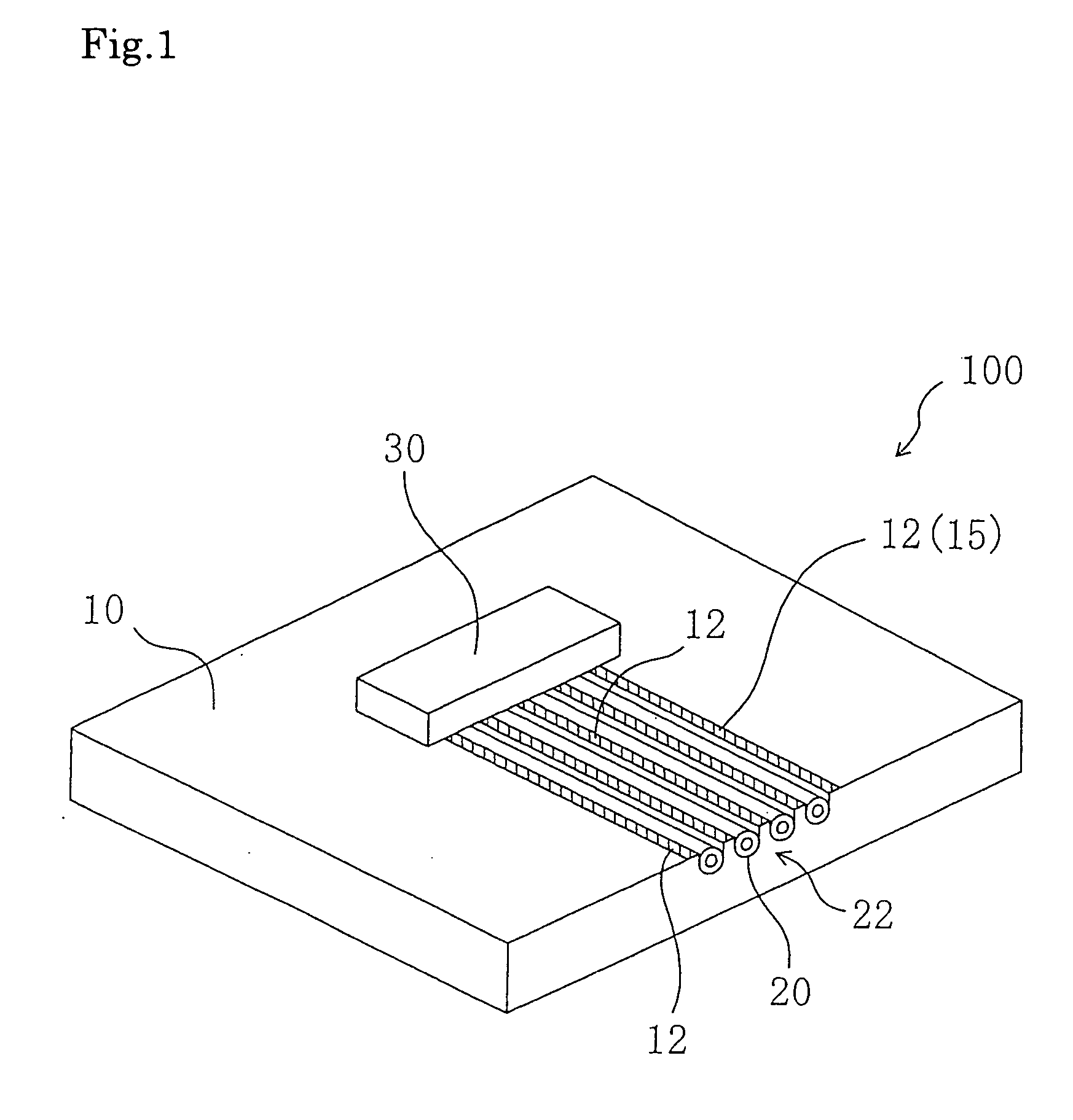
[0288]FIG. 1 is a perspective view schematically showing the configuration of an optical transmission channel board 100 of Embodiment 1.

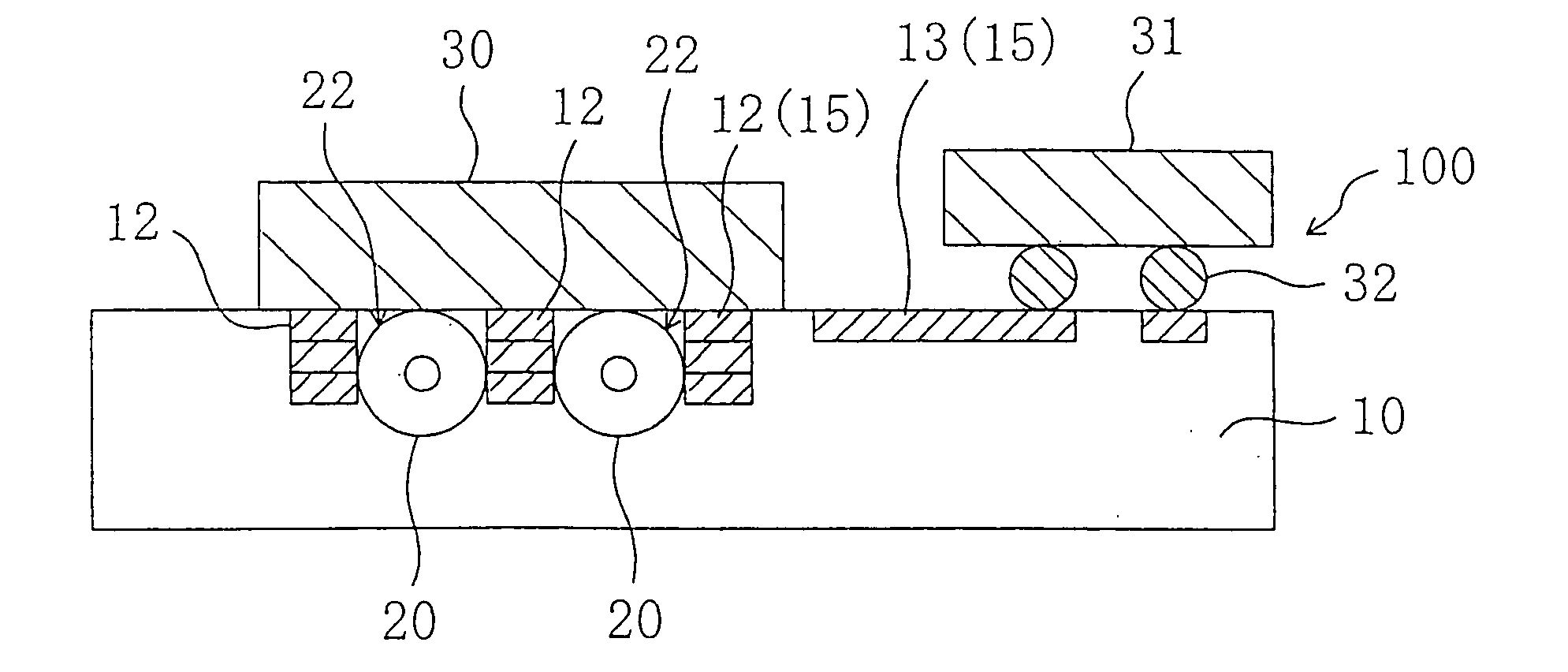
[0289] As shown in FIG. 1, the optical transmission channel board 100 of Embodiment 1 comprises: a board 10; and circuit patterns 15 including a plurality of wirings 12 formed on the board 10. A plurality of optical fibers 20 are arranged between each the wiring 12 of the circuit patterns 15, respectively. An optical transmission channel of the present invention indicates an optical fiber 20 of Embodiment 1. Thus, Embodiment 1 is described for the case of optical fibers. However, an “optical transmission channel” in the present specification indicates a line-shaped member capable of transmitting light. This holds also in the other embodiments described below.

[0290] When viewed from the abov...

Example

Embodiment 2

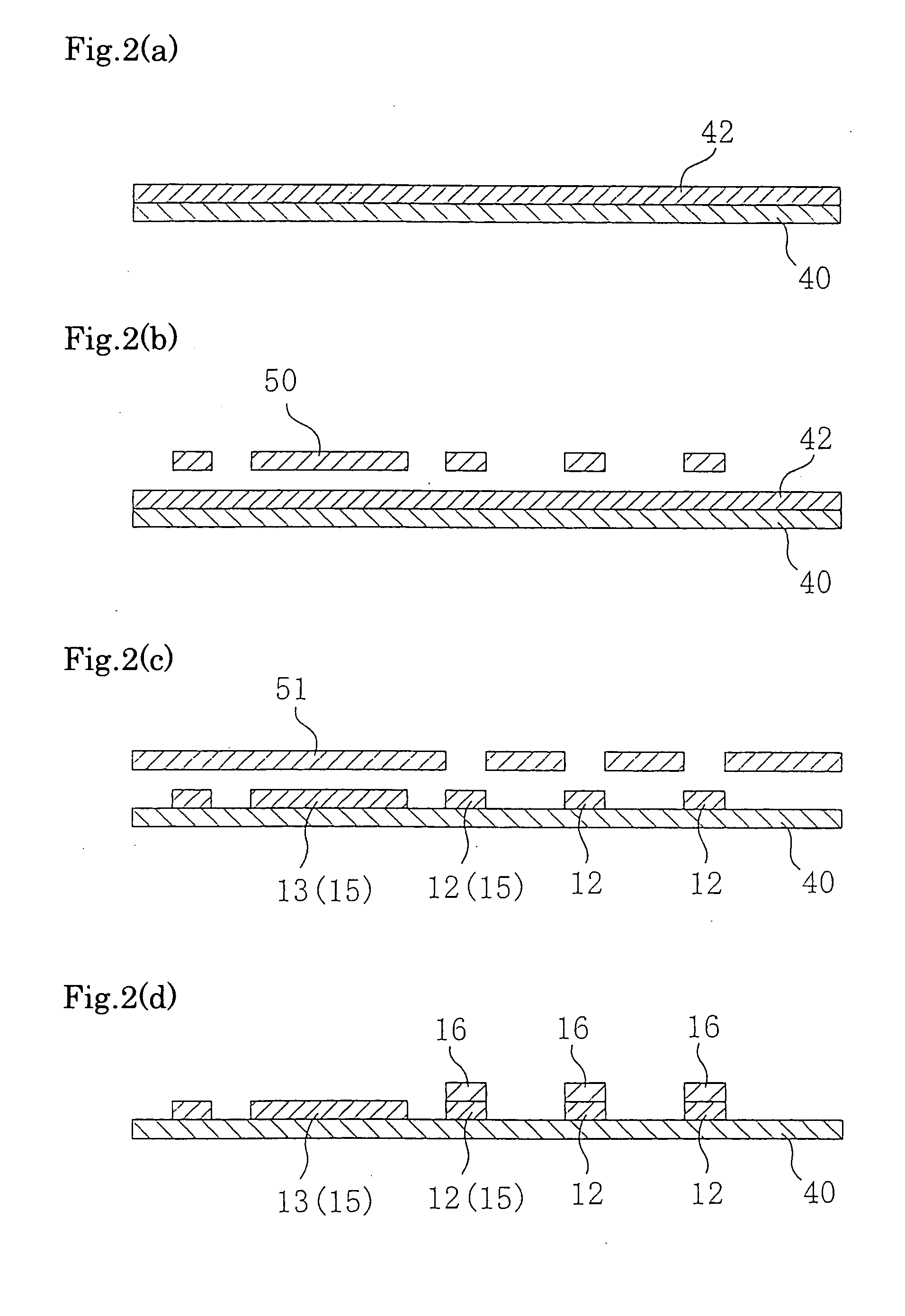
[0332] A fabrication method for an optical transmission channel board according to Embodiment 2 is described below. FIGS. 13(a)-13(e) are sectional views of an optical transmission channel board used for describing a fabrication method for an optical transmission channel board according to Embodiment 2.

[0333] First, starting from the state shown in FIG. 2(a), guide layers 16 and 17 are stacked on a metal layer 42 so that the state shown in FIG. 13(a) is achieved. Then, as shown in FIG. 13(b), these layers (17, 16, 42) are etched using a mask 53 for defining the shape of circuit patterns 15. As a result, circuit patterns 15 are formed that include: wirings 12 for constituting grooves 22; other wirings 13; and an optical element marker for positioning an optical element.

[0334] Then, as shown in FIG. 13(c), the guide layers 16 and 17 on top of the wirings 13 are etched using a mask 54 for defining the shape of the wiring 13 portion. As a result of this etching, guide wal...

Example

Embodiment 3

[0379]FIG. 21 is a perspective view schematically showing the configuration of an optical transmission channel board according to Embodiment 3.

[0380] As shown in FIG. 21, the optical transmission channel board 200 of Embodiment 3 comprises: a board 110 composed of a material containing resin; a plurality of grooves 122 formed in the surface of the board 110; and optical fibers 120 a portion of each of which is embedded in each groove 122. Circuit patterns (not shown) including a plurality of wirings are formed on the board 110. In the configuration of Embodiment 3, apart of the circuit patterns and the grooves 122 into which the optical fibers 120 are embedded are formed in self-conformity with each other. This self-conformal formation is described later in further detail in a fabrication method for the optical transmission channel board 200.

[0381] The optical transmission channels of the present invention are optical fibers 120 in Embodiment 3, and hence Embodiment 3...


PUM


Abstract

A fabrication method for an optical transmission channel board includes a first step of forming on a substrate a layer containing an electrically conductive material, and a second step of patterning said layer containing an electrically conductive material formed on said substrate, and thereby forming circuit patterns at least a part of which is used as an electric circuit and at least a part of which positionally regulates an optical transmission channel.

Description

BACKGROUND OF THE INVENTION [0001] 1. Field of the Invention [0002] The present invention relates to a fabrication method for an optical transmission channel board, an optical transmission channel board, a board with built-in optical transmission channel, a fabrication method for a board with built-in optical transmission channel, and a data processing apparatus. [0003] 2. Related Art of the Invention [0004] With recent progress in optical communications and optical information processing, optical circuit mounting technology permitting high-density and economical integration of optical components is increasingly important, and so is the role that optical modules play. An example of a prior art optical module is shown in FIG. 50 (see JP-A-H8-78657). [0005] As shown in FIG. 50, a prior art optical module 1000 comprises a Si substrate (Si terrace) 1101, optical fibers 1102, and a semiconductor laser (optical element) 1105. Guide grooves (V grooves) 1104 a formed in the Si substrate 110...

Claims


Application Information

Patent Timeline
IPC IPC(8): G02B6/00G02B6/12G02B6/122G02B6/36G02B6/42H05K1/02
CPCG02B6/3608G02B6/3636G02B6/3668G02B6/3676H05K2203/167G02B6/4214G02B6/4249H05K1/0274G02B6/3692G02F1/1309G02F1/1336G02F2203/69
Inventor KARASHIMA, SEIJINAKATANI, SEIICHISUGAYA, YASUHIROASAHI, TOSHIYUKIICHIRYU, TAKASHI
Owner PANASONIC CORP
Why Eureka
Try Eureka