Scanning electron microscope device, evaluation point generating method, and program

Active Publication Date: 2012-05-03
HITACHI HIGH-TECH CORP
View PDF6 Cites 0 Cited by
  • Summary
  • Abstract
  • Description
  • Claims
  • Application Information

AI Technical Summary

Benefits of technology

[0019]According to the present invention, FOV's for picking up images of all device portions having electric characteristics can be set efficiently and in consequence, highly accurate measurements can be realized efficiently.
[0020]The present invention pertains to a technique, according to which in respect of a device that is unknown, from only the layout design information, as to its portion where it has electric characteristics, the portion having electric characteristics is identified and FOV's can be arranged efficiently (without causing an overlapping part as far as possible) at the portion. For example, in the invention, by using device constituent information and linking information possessed by the semiconductor design data prepared by using an EDA (Electronic Design Automation) tool, a recipe including patterns on semiconductor device necessary for verification of electric characteristics (evaluation points) is generated automatically.
[0021]Embodiments of the present invention will now be described with reference to the accompanying drawings. It should however be noted that the present embodiment is a mere example of realizing the present invention and does not limit the technical scope of the invention.

Problems solved by technology

For this reason, during transfer of a pattern to a wafer, rays of light for nearby patterns interfere with each other through a phenomenon called OPE (Optical Proximity Effect), bringing about a problem that patterns different from those of the rectile are transferred onto the resist.

Method used


Image

  • Scanning electron microscope device, evaluation point generating method, and program
  • Scanning electron microscope device, evaluation point generating method, and program
  • Scanning electron microscope device, evaluation point generating method, and program

Examples


Embodiment Construction

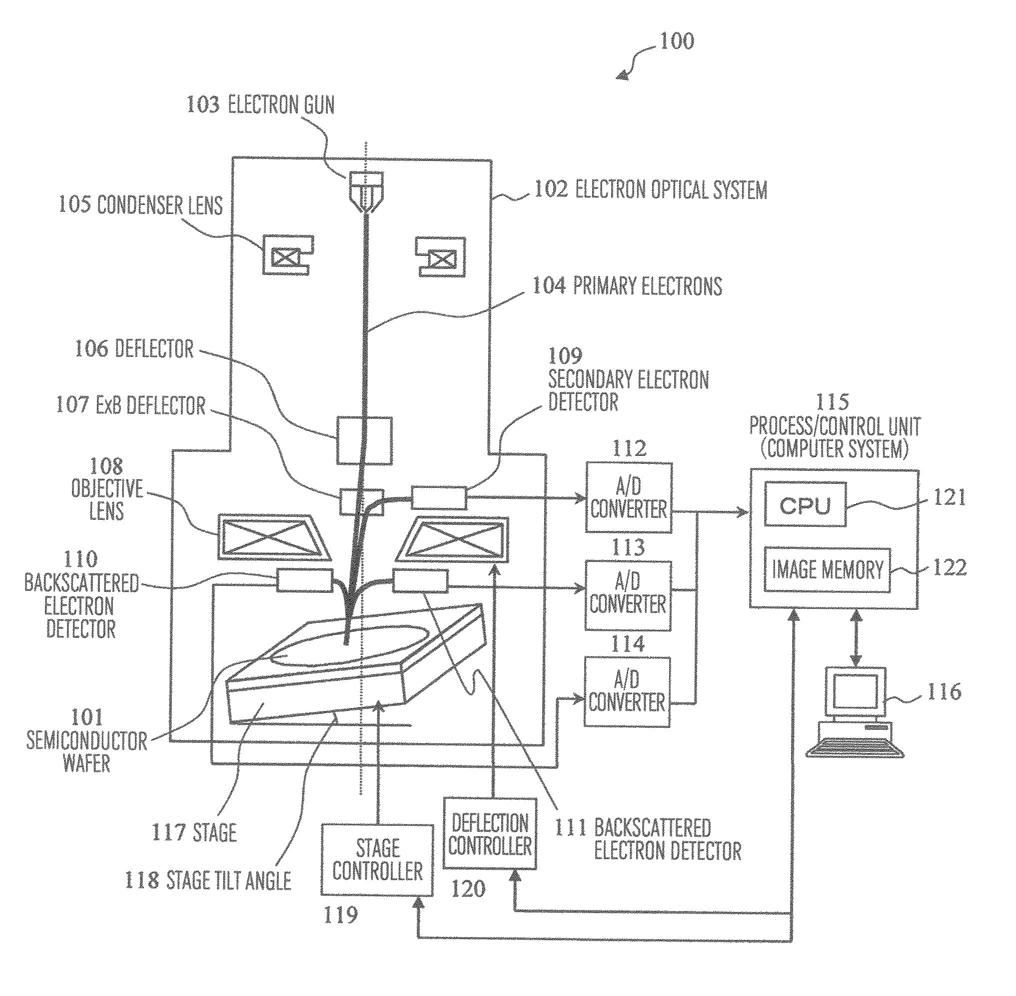
[0037]FIG. 1 is a block diagram illustrating schematic construction of a scanning electron microscope (SEM) for capturing a secondary electron image (SE image) or a backscattered electron image (BSE image) of a sample according to an embodiment of the present invention. It is to be noted that the SE image and the BSE image will hereinafter be generally called an SEM image. Then, it is assumed that the image captured here includes part or all of a top / down image obtained by observing a measuring objective in vertical direction and a tilt image obtained when the measuring objective is observed in a direction at an arbitrary inclination angle.

[0038]In FIG. 1, 103 designates an electron gun adapted to generate an electron beam 104. In order that the electron beam is focused and irradiated on a desired position on a semiconductor wafer 101 representing a sample mounted on a stage 117, the landing position of electron beam and an aperture therefore are controlled by means of a deflector 1...


PUM


Abstract

An image acquisition condition necessary to so arrange FOV's as not to overlap along a device shape so that all constituent arreas necessary for electric characteristic measurement may be confined in the FOV's is determined from device shape information (including circuit design data and layout design data) possessed by CAD data. Since, contingently upon the shape of a wiring portion, the wiring portion of a device is expressed by using a plurality of basic constituent figures in combination, a process of arranging FOV's to the individual constituent figures is executed. For a cell portion, a FOV is arranged in reference to a cell outer frame and apexes. At that time, any apex is a starting point of the FOV arrangement process and another apex is an end point of the same process.

Description

TECHNICAL FIELD[0001]The present invention relates to generation of a recipe for performing measurement of a finished shape of a semiconductor device, especially, measurement of evaluation points by using a scanning electron microscope.BACKGROUND ART[0002]When forming a device or a wiring pattern in a semiconductor wafer, a method is adopted in which a coating substance called resist is coated on the semiconductor wafer, a light exposure mask of a pattern shape (reticule) is overlaid on the resist, and the resist is exposed to light by exposing such light as visual rays / ultraviolet rays from above the reticle, thus forming the pattern. The thus obtained pattern will change in its shape contingently upon the intensity of an irradiated electron beam or the aperture and therefore, for formation of a highly accurate pattern, the workmanship of the pattern needs to be inspected.[0003]For inspection of such a pattern as above, a critical dimension scanning electron microscope (CD-SEM) has...

Claims


Application Information

Patent Timeline
IPC IPC(8): H01J37/26G01N23/00
CPCH01J37/28H01J2237/2817H01J2237/24592H01J37/3023
Inventor KAWASAKI, TAKAHIRO
Owner HITACHI HIGH-TECH CORP
Why Eureka
Try Eureka