Method for transferring a layout of an integrated circuit level to a semiconductor substrate

Inactive Publication Date: 2005-09-08
INFINEON TECH AG
View PDF7 Cites 8 Cited by
  • Summary
  • Abstract
  • Description
  • Claims
  • Application Information

AI Technical Summary

Benefits of technology

[0025] This alternative embodiment of the invention is based on the concept, as a modification in comparison with the first alternative, of omitting the step of filling the connecting space via dark regions. This inevitably results in phase edges in the region of the connecting space, depending on the extent to which the areas of the spaces that have been acted upon in respect of phase project beyond these into the connecting space. The effect of the

Problems solved by technology

Techniques adapted to a specific structure arrangement within the layout or the pattern correspondingly formed on the mask may exhibit no effect or a disadvantageous effect on an adjacent structure arrangement in the same layout or pattern.
A structure-shared process window that results overall for the imaging may be adversely impaired.
However, this in turn results in a dramatically reduced wafer throughput and, consequently, significantly higher costs in the area of lithography and for

Method used


Image

  • Method for transferring a layout of an integrated circuit level to a semiconductor substrate
  • Method for transferring a layout of an integrated circuit level to a semiconductor substrate
  • Method for transferring a layout of an integrated circuit level to a semiconductor substrate

Examples


Embodiment Construction

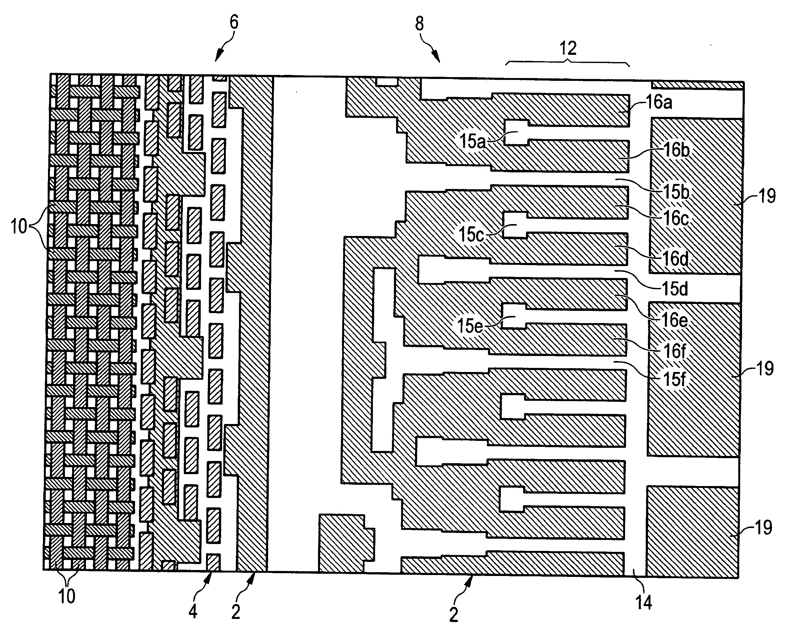
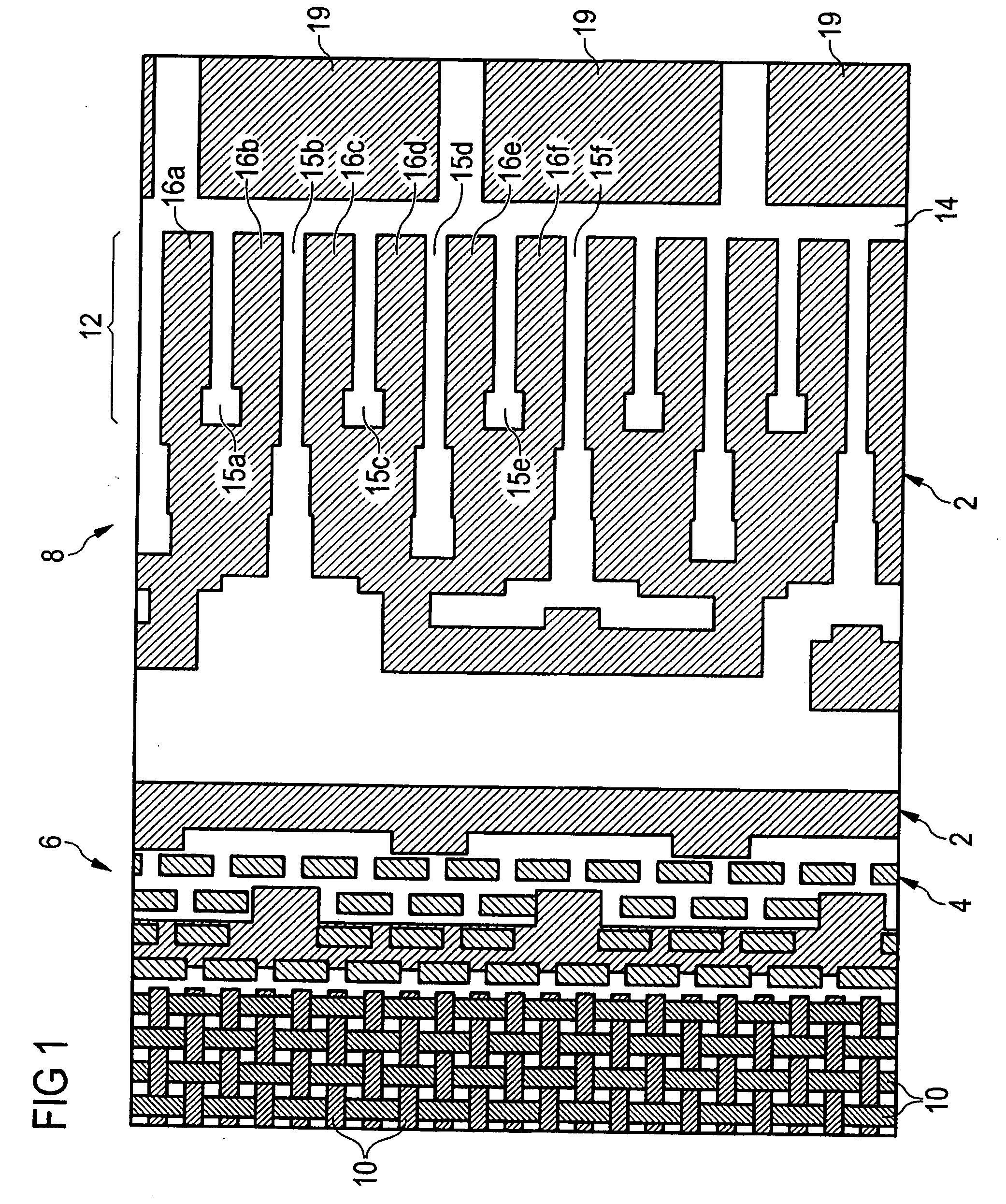
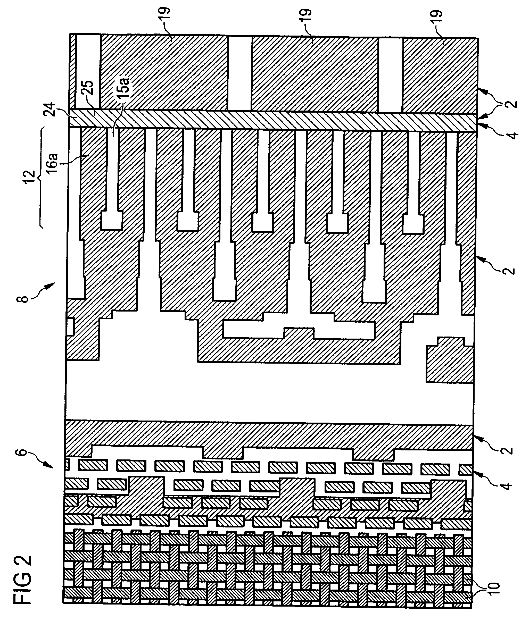
[0035] An exemplary embodiment of the invention will be explained on the basis of an AA mask level used for fabricating a memory chip. The memory chip is embodied using trench capacitor technology.

[0036]FIG. 1 shows a detail from a first layout 2 and a second layout 4, superimposed with the latter, from the edge of the memory cell array 6 (left-hand side of FIG. 1) with an adjoining periphery, the so-called support structures 8 (right-hand side). The first layout 2 represents the pattern of active regions that is to be imaged conventionally via an AA mask level on the semiconductor substrate. In the figures, regions of the AA mask level that are to be fabricated in an opaque or semitransparent fashion, that is to say light-shading to a greater or lesser extent on the mask, are illustrated with a gray background, while the essentially transparent spaces are shown white.

[0037] The superimposed second mask layout 4 represents the DT mask level. It solely comprises the structure eleme...


PUM


Abstract

A mask level layout has an arrangement of lines and spaces with the spaces interconnected by a further space. The spaces are alternately acted upon with a phase deviation with respect to the spaces, where a phase edge between spaces acted upon differently arises in the region of the further space. Alternatively, the connecting space within the layout may be filled with dark regions. An additional space is inserted in a second layout representing a further mask of the same mask set. The additional space enables formation of an insulating region on a semiconductor substrate at the location where formation of a continuous isolation trench is not possible due to the phase edges or dark regions within originally connecting spaces of the first mask. The first mask can be embodied as a hybrid mask with structures according to the principle of alternating phase masks with a large process window.

Description

CROSS REFERENCE TO RELATED APPLICATIONS [0001] This application claims priority under 35 USC §119 to German Application No. DE 102004010902.8, filed on Mar. 5, 2004, and entitled “Method for Transferring a Critical Layout of a Level of an Integrated Circuit to a Semiconductor Substrate,” the entire contents of which are incorporated herein by reference. FIELD OF THE INVENTION [0002] The present invention relates to a method for transferring a critical layout of an integrated circuit level to a semiconductor substrate. The layout includes an arrangement of spaces in the vicinity of regions to be formed in an opaque or semitransparent fashion on a mask. The spaces are connected to one another by a further space provided laterally with respect to the arrangement. The arrangement may further be periodic. BACKGROUND OF THE INVENTION [0003] In order to be able to achieve further advances in miniaturization in semiconductor technology, in particular in semiconductor memories, it is necessa...

Claims


Application Information

Patent Timeline
IPC IPC(8): G03F1/30G03F7/20G03F9/00
CPCG03F1/30G03F7/70433G03F7/70466
Inventor NOLSCHER, CHRISTOPHPFORR, RAINERHENNIG, MARIOKIESLICH, ALBRECHT
Owner INFINEON TECH AG
Why Eureka
Try Eureka