

Electronic component having an integrated passive electronic component and associated production method
- Summary
- Abstract
- Description
- Claims
- Application Information
AI Technical Summary
Benefits of technology
Problems solved by technology
Method used
Image

Examples
Embodiment Construction
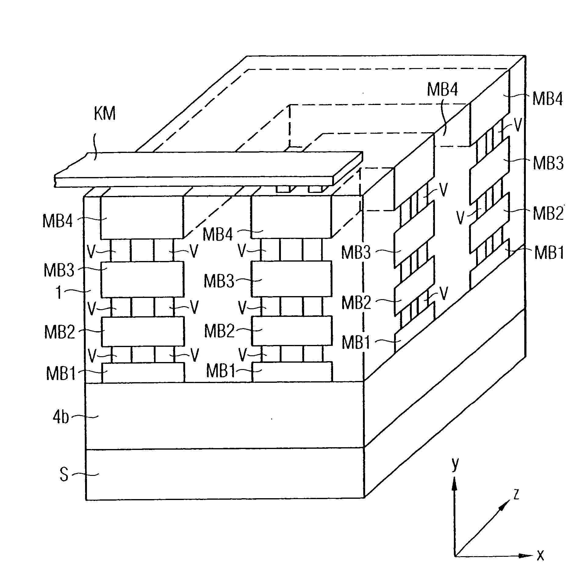
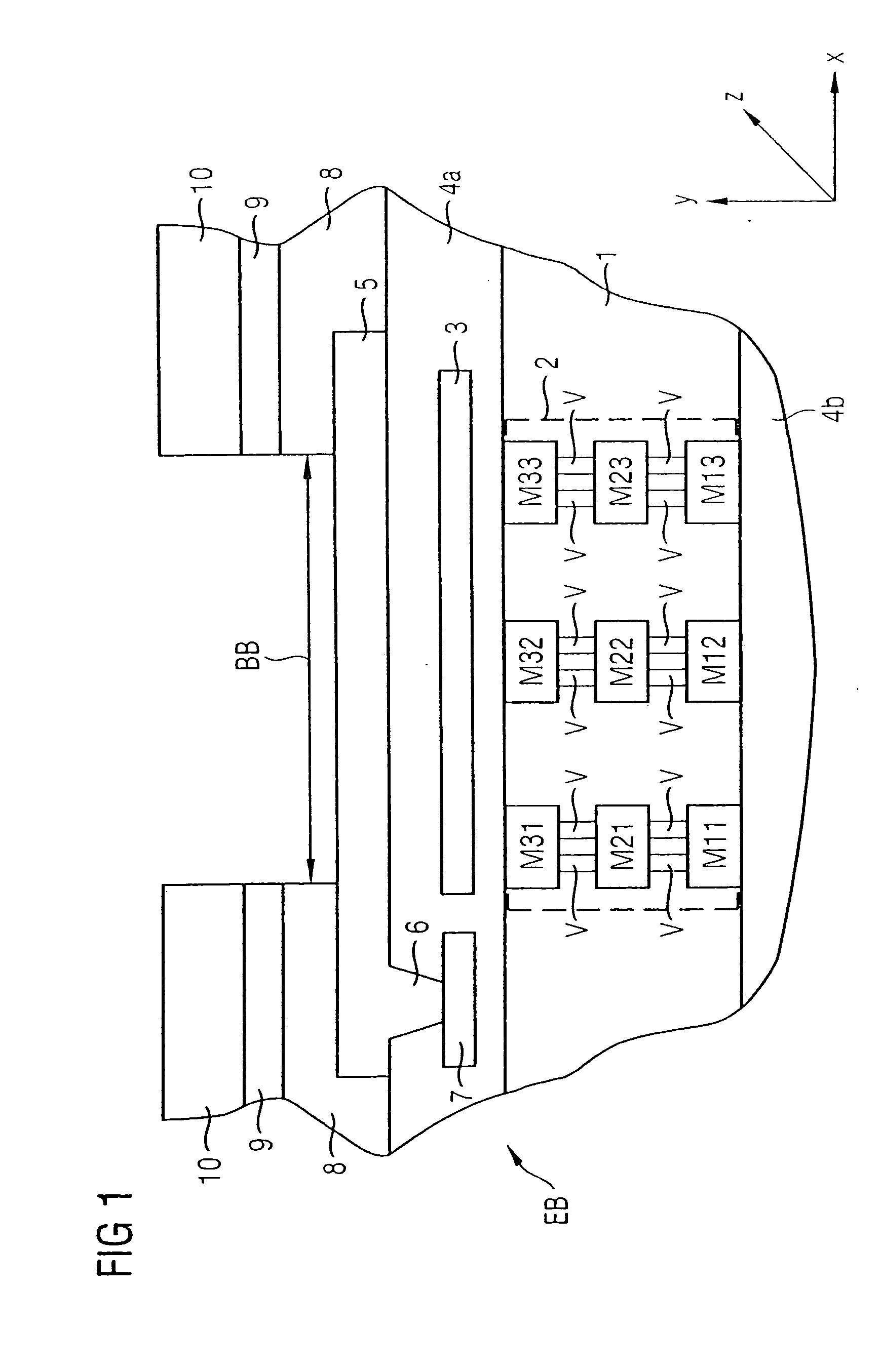
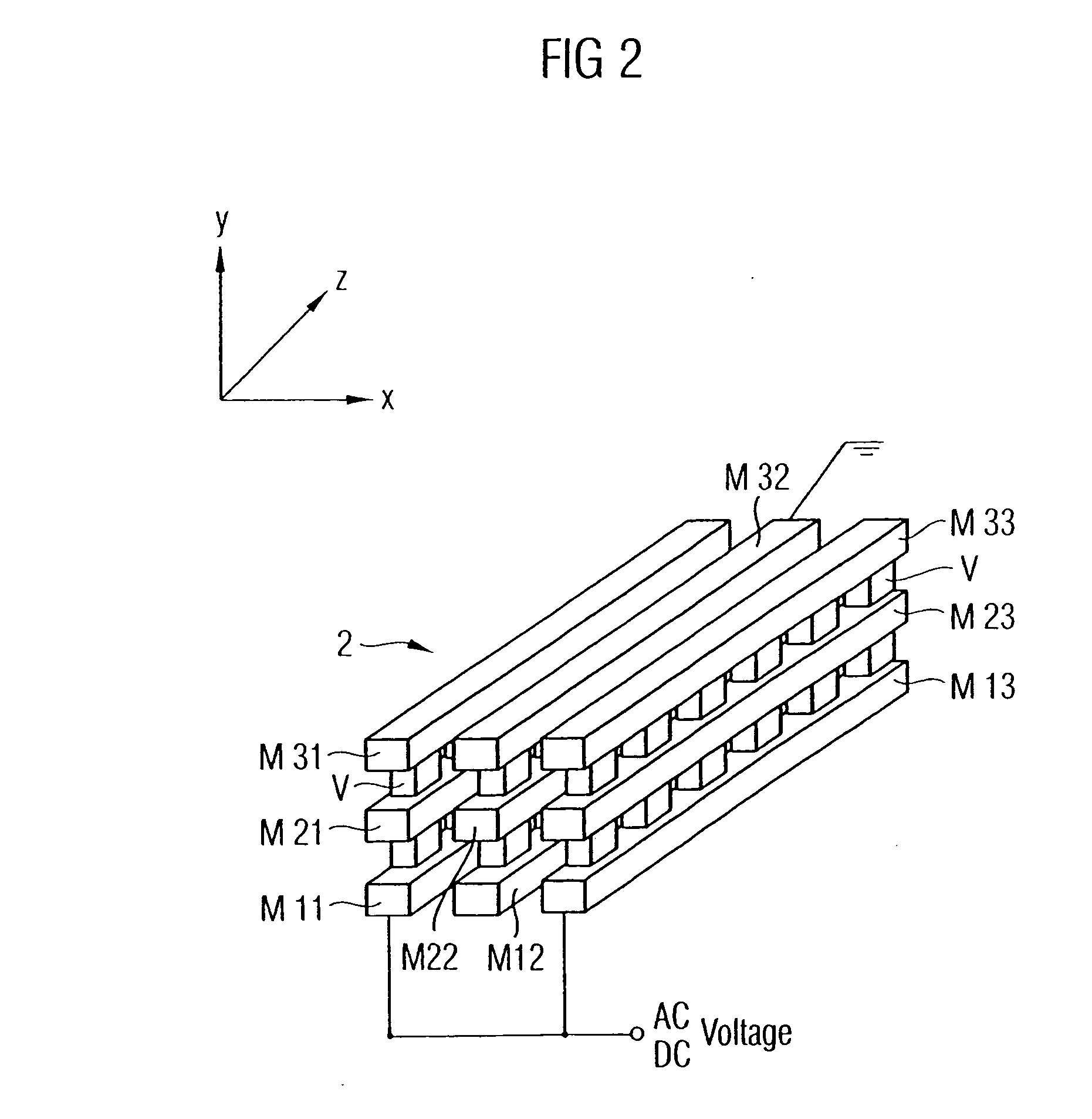
[0034] An electronic component EB (FIG. 1) has a first insulation layer 1 is formed from a material having a low dielectric constant. An electrically conductive structure 2 is integrated in this first insulation layer 1. The electrically conductive structure 2 is formed as a capacitance structure and is constructed from the metal strips M11 to M33. The metal strips M11 to M33 extend in the z direction parallel to one another, the metal strips M11 to M13, the metal strips M21 to M23 and the metal strips M31 to M33 in each case being formed in a metallization plane. The metal strips M11, M21 and M31 are arranged congruently with respect to one another and are electrically connected to one another by means of via connections V. This also applies analogously to the metal strips M12, M22 and M32 and also M13, M23 and M33. The metal strips M11, M21 and M31 and also M13, M23 and M33 are connected to a supply voltage potential either a DC or an AC voltage. The metal strips M12, M22 and M32 ...
PUM
 Abstract
Description
Claims
Application Information