Differential pressure sensor

a pressure sensor and differential technology, applied in the direction of fluid pressure measurement, acceleration measurement using interia forces, instruments, etc., can solve the problems of relatively complex surface micromechanical methods, and achieve the effects of reducing costs, stable diaphragm attachment, and simplifying manufacturing processes

Inactive Publication Date: 2005-09-15
ROBERT BOSCH GMBH
View PDF5 Cites 25 Cited by
  • Summary
  • Abstract
  • Description
  • Claims
  • Application Information

AI Technical Summary

Benefits of technology

[0011] Particularly advantageous is the production of the cavity using the trench etch process starting from the back of the semiconductor substrate. The buried and oxidized porous layer may be used as an etch stop layer for the trench etch process. The removal of the etch-stop layer may be avoided by using the oxidized porous first layer as a diaphragm layer or part of the diaphragm layer. In addition to reducing costs, this also simplifies the manufacturing process, because no method steps for removing the etch stop material are needed.
[0012] In another example embodiment of the present invention, the lateral dimension of the porous first layer is greater than the lateral dimension of the cavity. Etching through the semiconductor substrate in the trench etch process may thus be avoided. This results in a stable attachment of the diaphragm. The lateral tolerances in trench etching may be compensated.
[0013] The trench etch process starting from the back of the semiconductor substrate may be advantageously controlled by the flanks of the cavity having a negative flank angle, for example. Micropassivation by oxygen precipitates, for example, is thus prevented.

Problems solved by technology

These surface micromechanical methods are relatively complex due to the need for separate sacrificial layers.

Method used


Image

  • Differential pressure sensor
  • Differential pressure sensor
  • Differential pressure sensor

Examples


Embodiment Construction

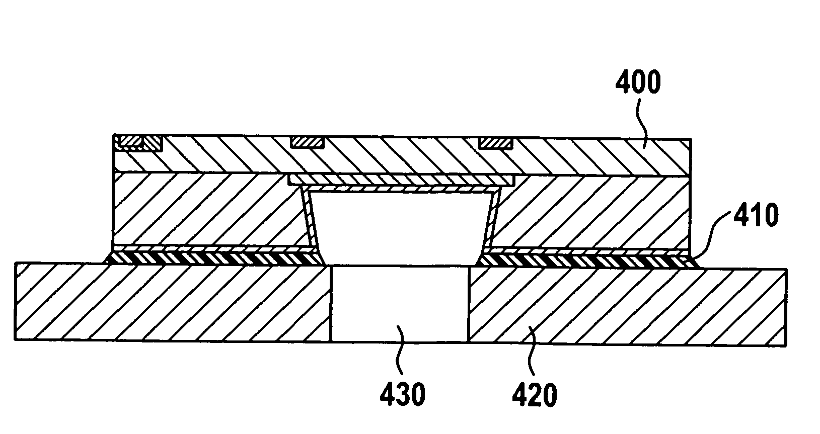
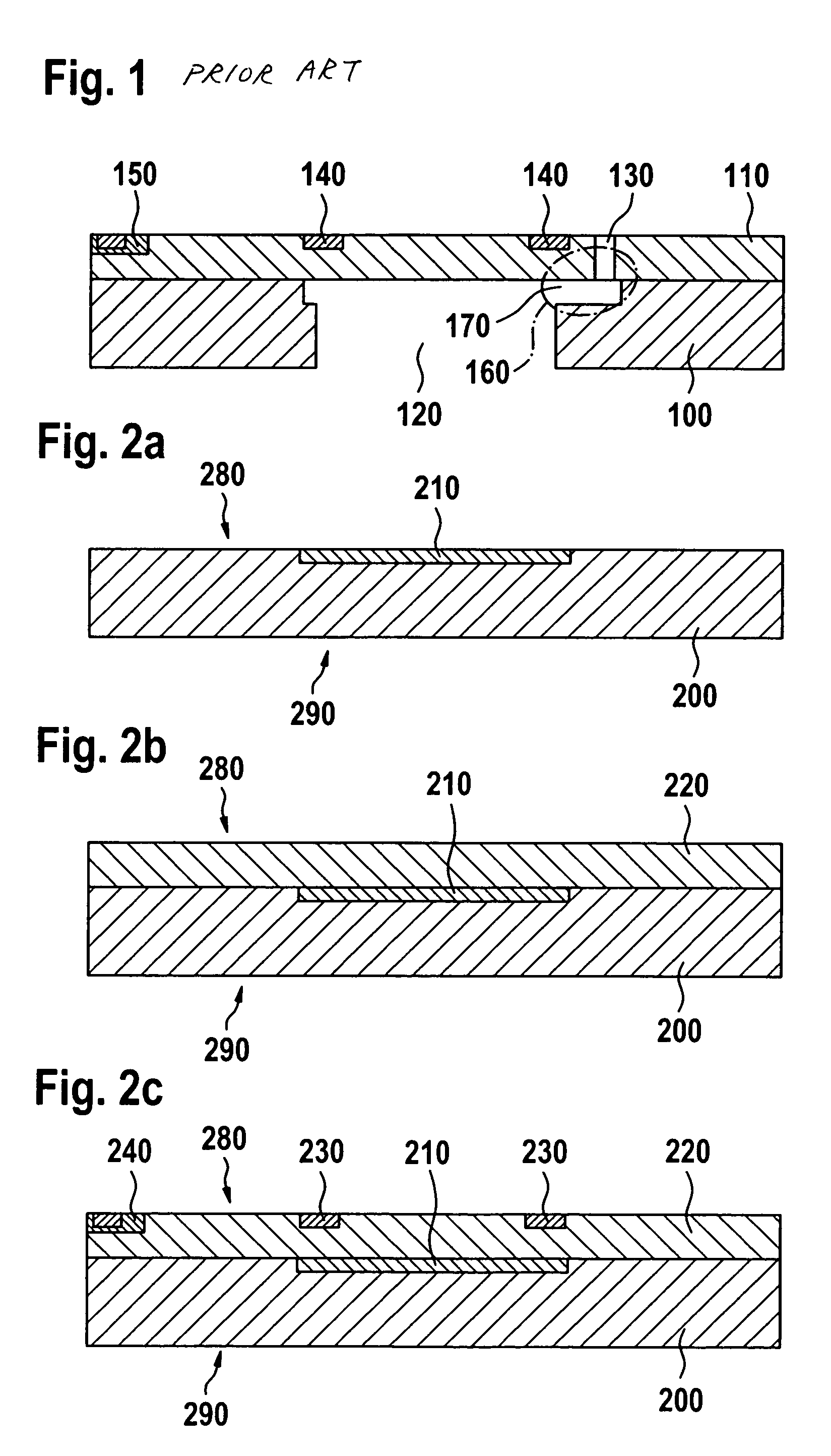
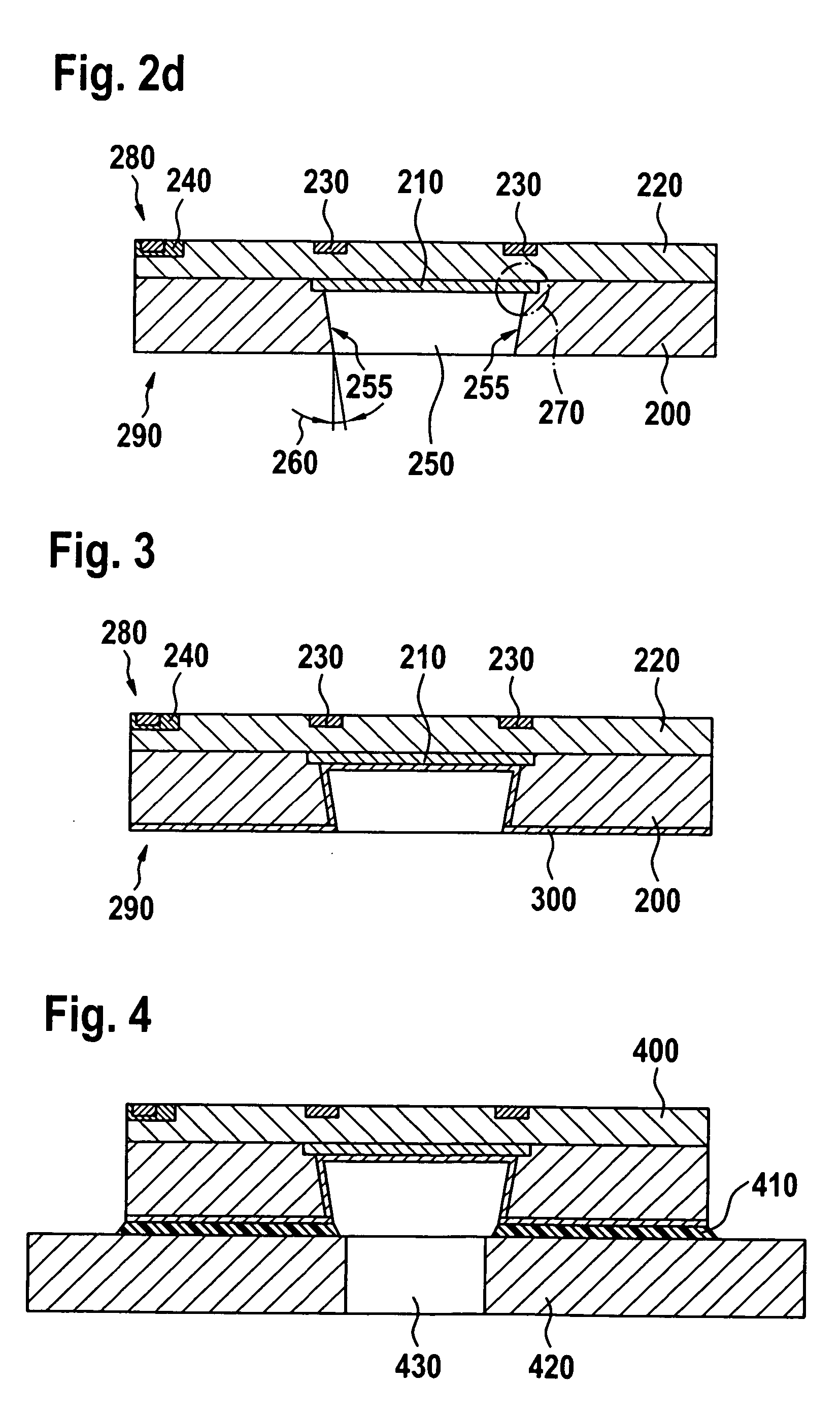
[0022]FIG. 1 illustrates a conventional micromechanical pressure sensor known in the art. An epitaxial layer 110, which forms a diaphragm over a cavity 120, is applied to a semiconductor substrate 100. Piezosensitive resistors 140, which convert the movement of the diaphragm in the event of a pressure difference between the medium in cavity 120 and the outside into a detectable pressure quantity, are applied to epitaxial layer 110. In addition, at least part of an analyzer circuit 150 for processing the pressure quantity may be mounted on epitaxial layer 110. Normally, part of cavity 120 is produced via a porous layer which, in the subsequent manufacturing process, is removed from the front of the pressure sensor through an appropriate access opening 130. In such a manufacturing process, in the subsequent trench opening from the back of the substrate, a circumferential gap 170 is formed at the level of the original porous layer as illustrated by area 160 in FIG. 1. When using such a...


PUM

PropertyMeasurementUnit
thickaaaaaaaaaa
areaaaaaaaaaaa
lateral dimensionaaaaaaaaaa

Abstract

In a method for manufacturing a micromechanical semiconductor component, e.g., a pressure sensor, a locally limited, buried, and at least partially oxidized porous layer is produced in a semiconductor substrate. A cavity is subsequently produced in the semiconductor substrate from the back, directly underneath the porous first layer, using a trench etch process. The porous first layer is used as a stop layer for the trench. Thin diaphragms having a low thickness tolerance may thus be produced for differential pressure measurement.

Description

FIELD OF THE INVENTION [0001] The present invention is directed to a micromechanical semiconductor component and a method for manufacturing a micromechanical component. BACKGROUND INFORMATION [0002] Semiconductor components, in particular diaphragm sensors and methods for manufacturing diaphragm sensors on the basis of semiconductor substrates, silicon wafers, for example, are known. A flat porous diaphragm area, for example, is placed on a semiconductor substrate as a substrate layer for sensor structures, and subsequently a clearance for insulating, e.g., thermally, the diaphragm is produced by removing the porous layer (sacrificial layer) underneath the diaphragm. [0003] The conventional diaphragm sensors are mostly implemented as thin-layer diaphragm sensors. Initially layer systems having a thickness between tens of nanometers and a few μm are deposited onto a substrate, whereupon the substrate is removed in predefined areas to obtain unsupported diaphragm areas. Sensor structu...

Claims


Application Information

Patent Timeline
Patent Type & Authority Applications(United States)
IPC IPC(8): B81B3/00B81C1/00G01L9/00H01L21/00H01L29/84
CPCB81C1/00158B81B2201/0264G01L9/0054B81C2201/014G01L9/0042B81C2201/0115
Inventor BENZEL, HUBERTLAMMEL, GERHARD
Owner ROBERT BOSCH GMBH
Why Eureka
Try Eureka