Sealed integral mems switch

a mems switch and integral technology, applied in the field of radio frequency, can solve the problems of poor electrical isolation in the “off” and large insertion loss of solid-state switches, and achieve the effects of cost-effectiveness, easy manufacturing, and economical manufacturing

Inactive Publication Date: 2005-09-22
SIVERTA INC
View PDF22 Cites 59 Cited by
  • Summary
  • Abstract
  • Description
  • Claims
  • Application Information

AI Technical Summary

Benefits of technology

[0020] Another object of the present invention is to provide a MEMS switch which is simpler.
[0021] Another object of the present invention is to provide a MEMS switch that is cost effective.
[0022] Another object of the present invention is to provide a MEMS switch that is easy to manufacture....

Problems solved by technology

When RF signal frequency exceeds about 1 GHz, solid state switches suffer from large insertion loss in the “On” state (i.e., when an electrical ...

Method used


Image

  • Sealed integral mems switch
  • Sealed integral mems switch
  • Sealed integral mems switch

Examples


Embodiment Construction

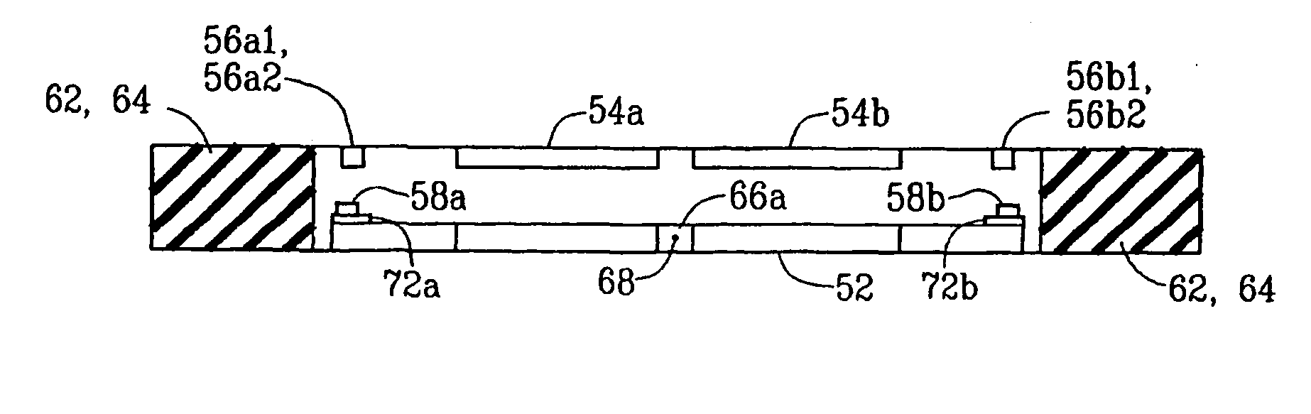
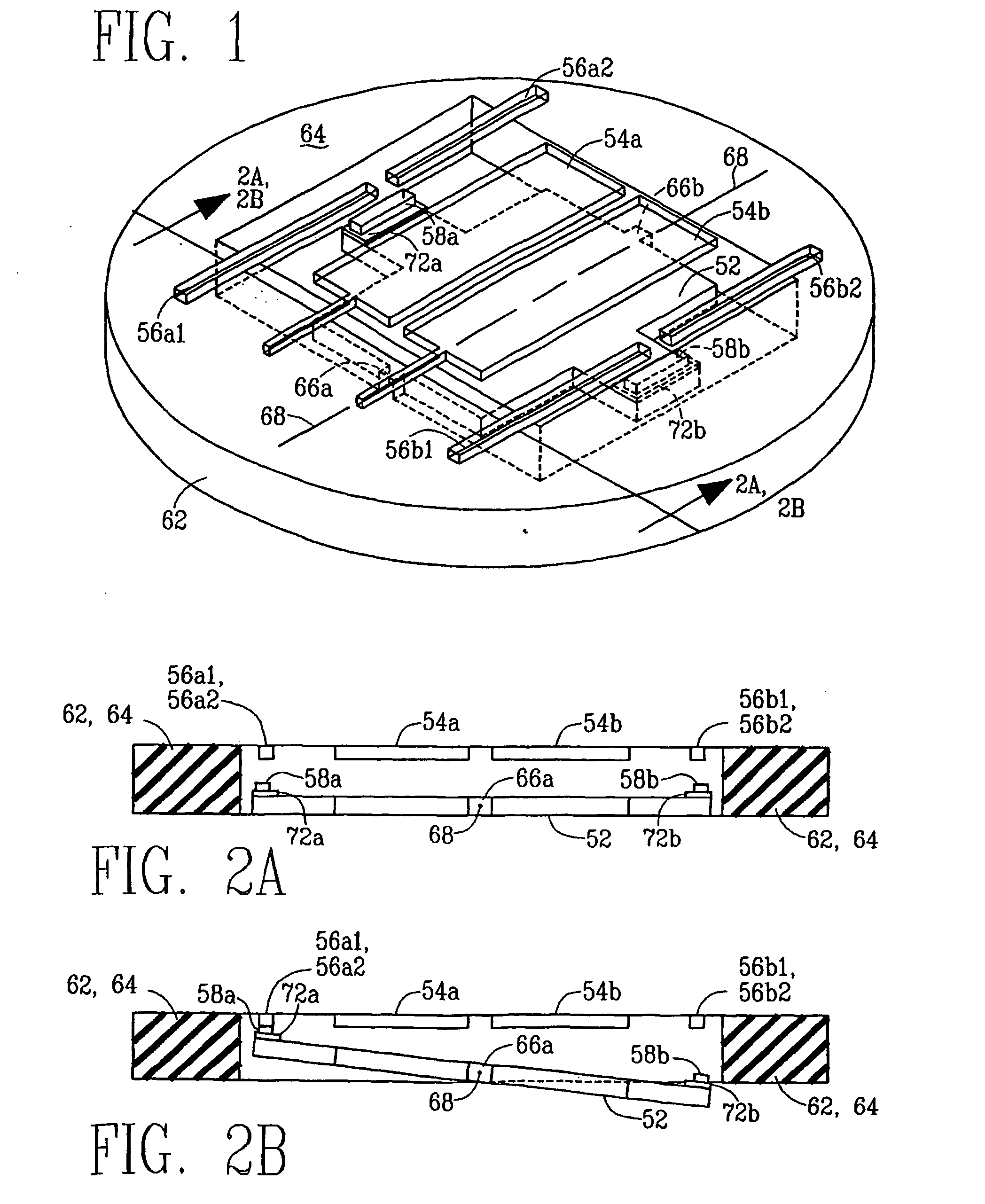
[0055]FIGS. 1, 2A and 2B illustrate a seesaw 52, metallic electrodes 54a and 54b, metallic switch contacts 56a1, 56a2, 56b1 and 56b2, and metallic shorting bars 58a and 58b that are included in MEMS switches of the present invention. The seesaw 52 is formed by micro-machining a layer 62 of material, preferably single crystal silicon (Si). Material of the layer 62 also forms a frame 64 which preferably surrounds the seesaw 52. A pair of torsion bars 66a and 66b, which are depicted by dashed lines in FIG. 1 and which extend outward from opposite sides of the seesaw 52 to the frame 64, are also formed monolithically with the seesaw 52 and the frame 64 from the material of the layer 62. While dimensions of the seesaw 52 vary depending upon a particular configuration for the MEMS switch, in one illustrative embodiment the aperture micro-machined into the layer 62 to establish the frame 64 which surrounds the seesaw 52 measures approximately about 0.4×0.4 millimeters. In this same illustr...


PUM


Abstract

A MEMS switch includes a micro-machined monolithic layer (122) having, a seesaw (52), a pair of torsion bars (66a, 66b), and a frame (64). The frame (64) supports the seesaw (52) for rotation about an axis (68) established by the torsion bars (66a, 66b). Shorting bars (58a, 58b) at ends of the seesaw (52) connect across pairs of switch contacts (56a1, 56a2, 56b1, 56b2) carried on a substrate (174) bonded to one surface of the layer (122). A base (104) is also joined to a surface of the layer (122) opposite the substrate (174). The substrate (174) carries electrodes (54a, 54b) for applying forces to the seesaw (52) urging it to rotate about the axis (68). An electrical contact island (152) supported at a free end of a cantilever (166) ensures good electrical conduction between ground plates (162a, 162b) on the layer (122) and electrical conductors on the substrate (174).

Description

[0001] The present invention relates generally to the technical field of electrical switches, and, more particularly, to micro-electro mechanical systems (“MEMS”) switches. BACKGROUND ART [0002] Radio frequency (“RF”) switches are used widely in microwave and millimeter wave transmission systems for antenna switching applications including beam forming phased array antennas. In general, such switching applications presently use semiconductor solid state electronic switches, such as Gallium Arsenide (“GaAs”) MESFETs or PIN diodes, as contrasted with mechanical switches. Such semiconductor solid state electronic switches also are used extensively in cellular telephones for switching between transmitting and receiving. [0003] When RF signal frequency exceeds about 1 GHz, solid state switches suffer from large insertion loss in the “On” state (i.e., when an electrical signal passes through the switch) and poor electrical isolation in the “Off” state (i.e., when the switch blocks transmi...

Claims


Application Information

Patent Timeline
IPC IPC(8): H01H59/00H01P1/10H01P1/12
CPCH01H59/0009H01P1/127H01H2059/0054B81B7/04H01H59/00
Inventor PASHBY, GARY JOSEPHSLATER, TIMOTHY G.
Owner SIVERTA INC
Why Eureka
Try Eureka