Method for growing a gate oxide layer on a silicon surface with preliminary n2o anneal

a gate oxide layer and silicon surface technology, applied in the direction of semiconductor devices, basic electric elements, testing/measurement of semiconductor/solid-state devices, etc., can solve the problem that the gate oxide layer of the prior art cannot sustain high-voltage operation conditions, and achieve superior reliability and improved electric characteristics.

Inactive Publication Date: 2005-09-22
NAN YA TECH
View PDF6 Cites 2 Cited by
  • Summary
  • Abstract
  • Description
  • Claims
  • Application Information

AI Technical Summary

Benefits of technology

[0009] Accordingly, it is the primary object of the present invention to provide a method for making a robust, high-quality gate oxide layer that has improved electric characteristics such as superior reliability at high voltage (up to 14V) operation conditions.

Problems solved by technology

However, the gate oxide layer of the prior arts cannot sustain high voltage operation conditions such as a high voltage of 14V or even higher.

Method used


Image

  • Method for growing a gate oxide layer on a silicon surface with preliminary n2o anneal
  • Method for growing a gate oxide layer on a silicon surface with preliminary n2o anneal
  • Method for growing a gate oxide layer on a silicon surface with preliminary n2o anneal

Examples


Embodiment Construction

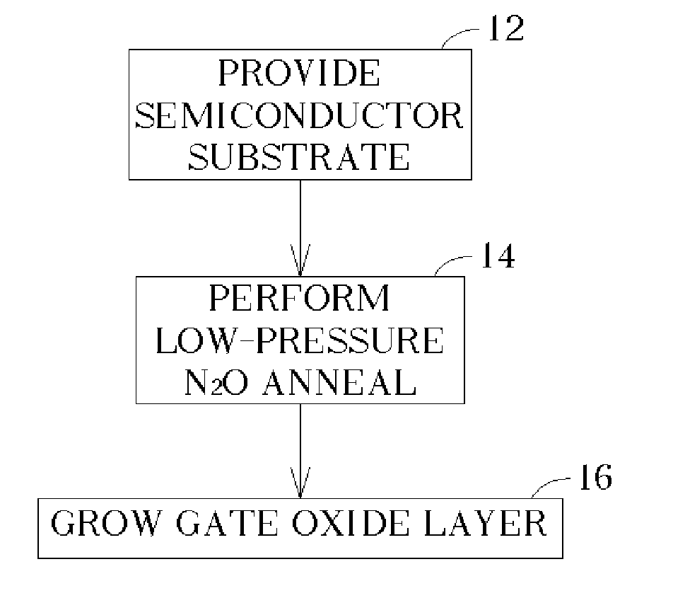
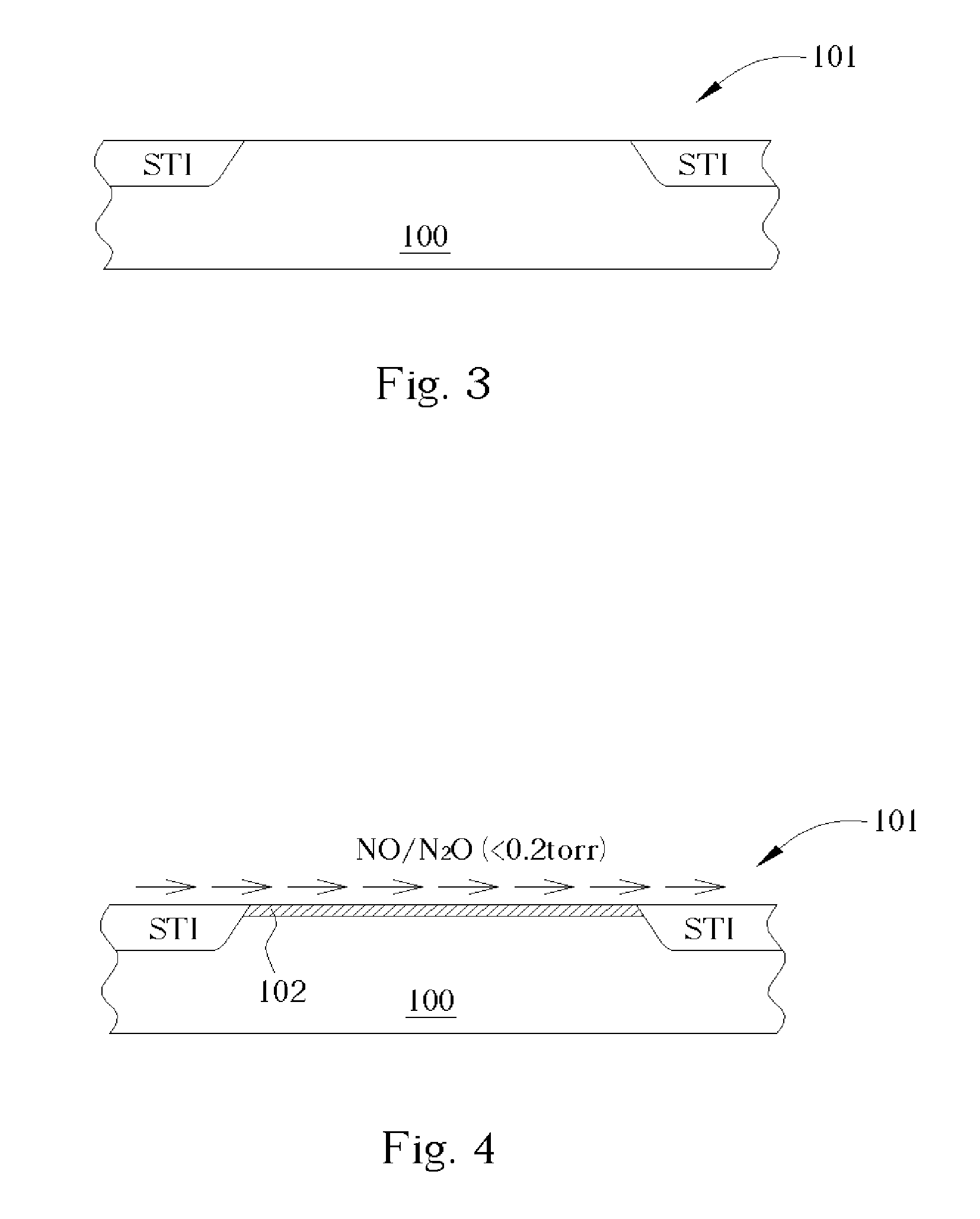
[0016] Please refer to FIG. 1. FIG. 1 is a flowchart illustrating a first preferred embodiment of the present invention. In Step 12, a semiconductor substrate such as a mono-crystalline silicon substrate is prepared. A plurality of silicon active areas that are isolated by device isolation structures are provided. Ordinarily, several cleaning procedures known in the art are carried out to obtain a clean silicon surface. After the cleaning process, a thin native oxide of few angstroms is formed on the silicon active areas. In Step 14, the semiconductor substrate is subjected to a preliminary anneal treatment. The preliminary anneal treatment is carried out in an airtight chamber. 10 sccm˜8000 sccm N2O gas is introduced into the chamber to maintain a low pressure of below 0.2 Torr. The anneal temperature is less than 1000° C. at a ramp rate of 5° C. / min to 100° C. / min. In Step 16, a high-quality gate oxide film is grown on the N2O pre-treated silicon surface (of the active areas) eith...


PUM


Abstract

The present invention relates to a method for growing a robust, high-quality gate oxide layer on a silicon surface. The resultant gate oxide layer made according to the present invention can pass the standard 50K times 14V high-voltage stress testing. The preferred embodiment of this invention includes a step of preliminary low-pressure N2O annealing that is carried out in an air-tight chamber at a temperature of less than 1000° C., a pressure below 0.2 torr, and N2O flow rate of below 8000 sccm. The preliminary low-pressure N2O annealing of the silicon surface is performed prior to the growth of high-quality gate oxide layer. In another preferred embodiment, N2O may be replaced with NO.

Description

BACKGROUND OF INVENTION [0001] 1. Field of the Invention [0002] The present invention relates to a method for growing a high-quality gate oxide layer on a silicon surface, and more particularly, to a method for growing a high-quality gate oxide layer with low-pressure N2O preliminary anneal. The gate oxide layer made according to the present invention method can sustain relatively higher voltage (up to 14V) than that made according to the prior art methods at the same thickness level. [0003] 2. Description of the Prior Art [0004] In the formation of integrated circuits on the surface of a semiconductor substrate, a gate oxide layer is typically grown over bare surface of a mono-crystalline substrate. The formation of this layer of stoichiometric and non-stoichiometric oxide is generally well known in the art. The gate oxide layer is preferably grown by means of thermal oxidation techniques. In the formation of for instance MOSFET devices, a polysilicon layer is deposited over the ga...

Claims


Application Information

Patent Timeline
Patent Type & Authority Applications(United States)
IPC IPC(8): G01R31/26H01L21/28H01L21/31H01L21/316H01L21/469H01L21/66
CPCH01L21/02238H01L21/02255H01L21/31662H01L21/2822H01L21/02312
Inventor LIN, SHIAN-JYH
Owner NAN YA TECH
Why Eureka
Try Eureka