
Integrated circuit

a technology of integrated circuits and circuits, applied in the field of integrated circuits, can solve the problems of significantly restricting the flexibility of test options, fewer bits available for test modes of operation in integrated circuits, and inability to route all of these control lines to the outside, so as to reduce the probability of a random or inadvertent activation of a test mode.

Inactive Publication Date: 2005-09-22
INTEL CORP
View PDF15 Cites 5 Cited by
  • Summary
  • Abstract
  • Description
  • Claims
  • Application Information

AI Technical Summary

Benefits of technology

[0018] The integrated circuit based on the present invention allows individual function blocks to be put into a test mode and allows these selected function blocks to be programmed with desired test data with little involvement. Hence, any desired combination of test mode and normal mode in a wide variety of function blocks is possible, for example, during the development which accompanies production.
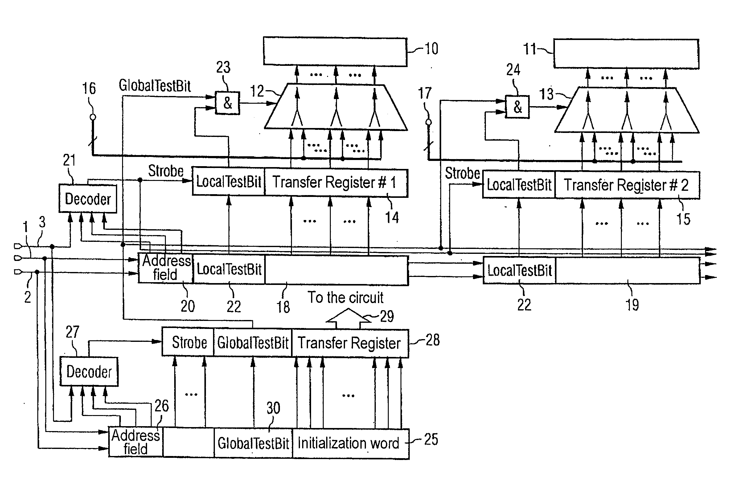
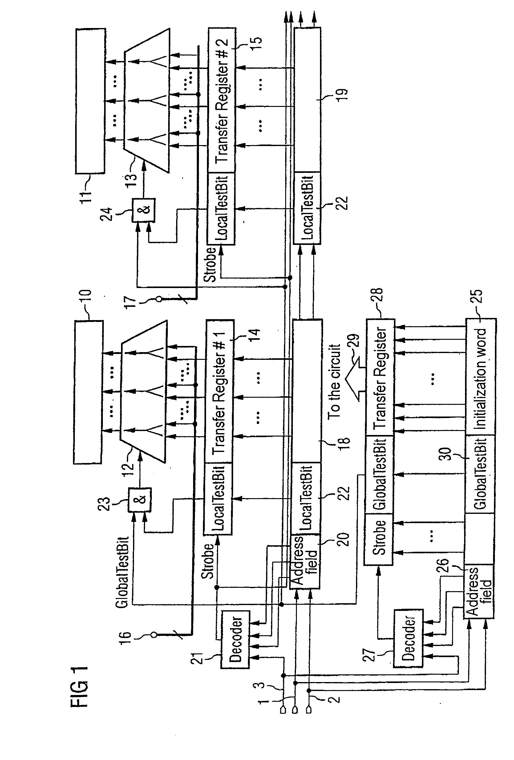
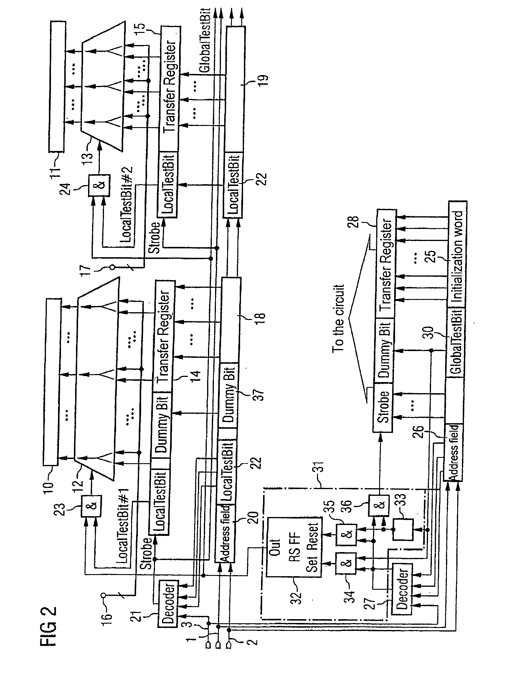
[0019] In one preferred embodiment of the present invention, the first and second test registers are coupled to one another in a series circuit in order to form a shift register chain. The formation of a shift register chain affords the advantage that just one address is needed to address all of the test registers. This saves scarce address space. The mode-of-operation memory cell associated with each test register means that the present invention still allows individual function blocks to be deliberately put into a test mode, while the remaining function blocks can operate in a normal mode. This ensures a further significant improvement in the flexibility in testing and the trial phase.
[0024] In line with a further, preferred embodiment, the control unit comprises a test mode-of-operation decoder which is coupled to a test register or to a further register, which is connected to the serial bus. In this case, the decoder is designed such that the state of a memory cell provided specifically for this purpose which indicates a global test mode is evaluated and actuates an AND gate, provided on every multiplexer, at an input. In this case, the output of the AND gate is connected to the changeover input of the associated multiplexer. By defining a global test mode of this type, which is precisely what allows a test mode for individual function blocks, the probability of a test mode being activated at random or inadvertently is significantly reduced.

Problems solved by technology

It is obvious that it is not possible to route all of these control lines to the outside.
The increasing complexity of the functions integrated on a chip, on the one hand, with the aim of setting a large number of operation-dependent parameters, and a limited number of address and data bits, on the other hand, mean that the bits which are available for test modes of operation in the integrated circuit are becoming fewer and fewer.
However, this requires additional, undesirable involvement during production and a further drawback in that the test options are significantly restricted in terms of flexibility.

Method used


Image

  • Integrated circuit
  • Integrated circuit
  • Integrated circuit

Examples


Embodiment Construction

[0030]FIG. 1 shows an integrated circuit which comprises two function groups, for example, namely a first function block 10 and a second function block 11. The first and second function blocks 10, 11 have a respective control input with a multiplicity of input connections, to which control commands, function parameters etc. can be supplied. The control inputs of the function blocks 10, 11 have the output of a respective multiplexer 12, 13 connected to them, with each input connection of the function blocks having a respective associated output connection on the multiplexers 12, 13, in the present case 20 connections for 20 parallel data bits. The first multiplexer 12 and the second multiplexer 13 each have a data input and a test input, between which it is possible to change over. The data input and the test input each comprise a number of input connections which corresponds to the output connections, in the present case 20 each.

[0031] The test inputs of the multiplexers 12, 13 are...


PUM


Abstract

The invention is directed to an integrated circuit that includes a plurality of functional circuit blocks. Respective associated multiplexers are used to change over between a normal mode and a test mode. The input side of the multiplexers each have a test register connected thereto which is coupled to a serial bus. A control unit controls the transfer of test data to a selected function block on the basis of the state of a mode-of-operation memory cell in the respective test register. This means that there is little involvement required to put individual function blocks of a chip deliberately into a test mode and to program them as appropriate, while other function blocks are operating in normal mode. The principle described allows a high degree of flexibility with regard to the testing of integrated circuits with a multiplicity of functional assemblies.

Description

REFERENCE TO RELATED APPLICATIONS [0001] This application is a continuation of PCT / DE03 / 02772, which was not published in English, that claims the benefit of the priority date of German Patent Application No. DE 102 41 385.1, filed on Sep. 6, 2002, the contents of which both are herein incorporated by reference in their entireties. FIELD OF THE INVENTION [0002] The present invention relates to an integrated circuit, and more particularly relates to a circuit having multiple function blocks that can be placed into a test mode independently of one another and which can be programmed using a serial bus. BACKGROUND OF THE INVENTION [0003] Integrated circuits are integrating more and more different functional units, with the scale of integration continually increasing. This means that, by way of example, the different transmission and receiver assemblies which need to be integrated into mobile radios are arranged in just one, fully integrated transceiver chip. This integrated circuit int...

Claims


Application Information

Patent Timeline
IPC IPC(8): G01R31/28G01R31/317G06F15/78
CPCG01R31/31701G06F15/7832G01R31/31723
Inventor GOSSMANN, TIMO
Owner INTEL CORP
Learn More