

Processing device and processing method
a processing device and processing method technology, applied in the direction of chemically reactive gases, crystal growth processes, coatings, etc., can solve the problems of reducing the speed of gas atmosphere change, difficult to carry out gas change in the area, and failing to achieve a sufficiently high productivity, etc., to achieve the effect of high speed
- Summary
- Abstract
- Description
- Claims
- Application Information
AI Technical Summary
Benefits of technology
Problems solved by technology
Method used
Image

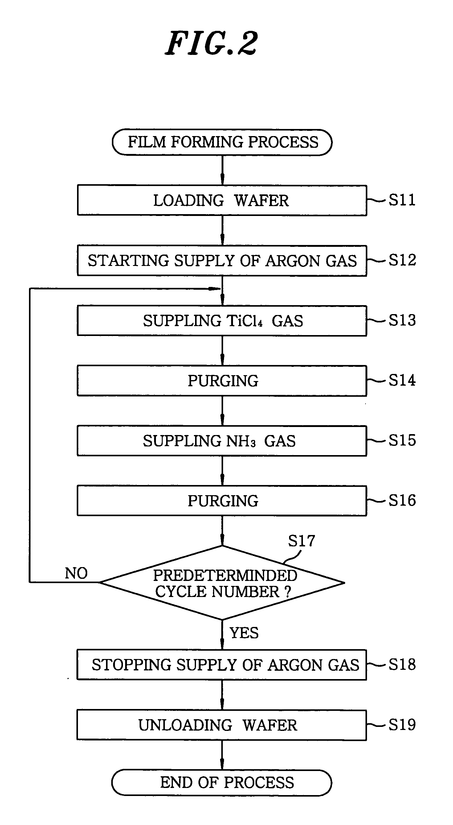
Examples
example
[0082]FIG. 3A illustrates a simulation result of a pressure distribution of the gas in the processing device shown in FIG. 1 in accordance with the preferred embodiment of the present invention. Further, FIG. 3B indicates a result of a case wherein a conventional chamber 12′ is employed (Comparison Example). The conditions of the simulation are as follows:
Preferred Embodiment of the Present Invention
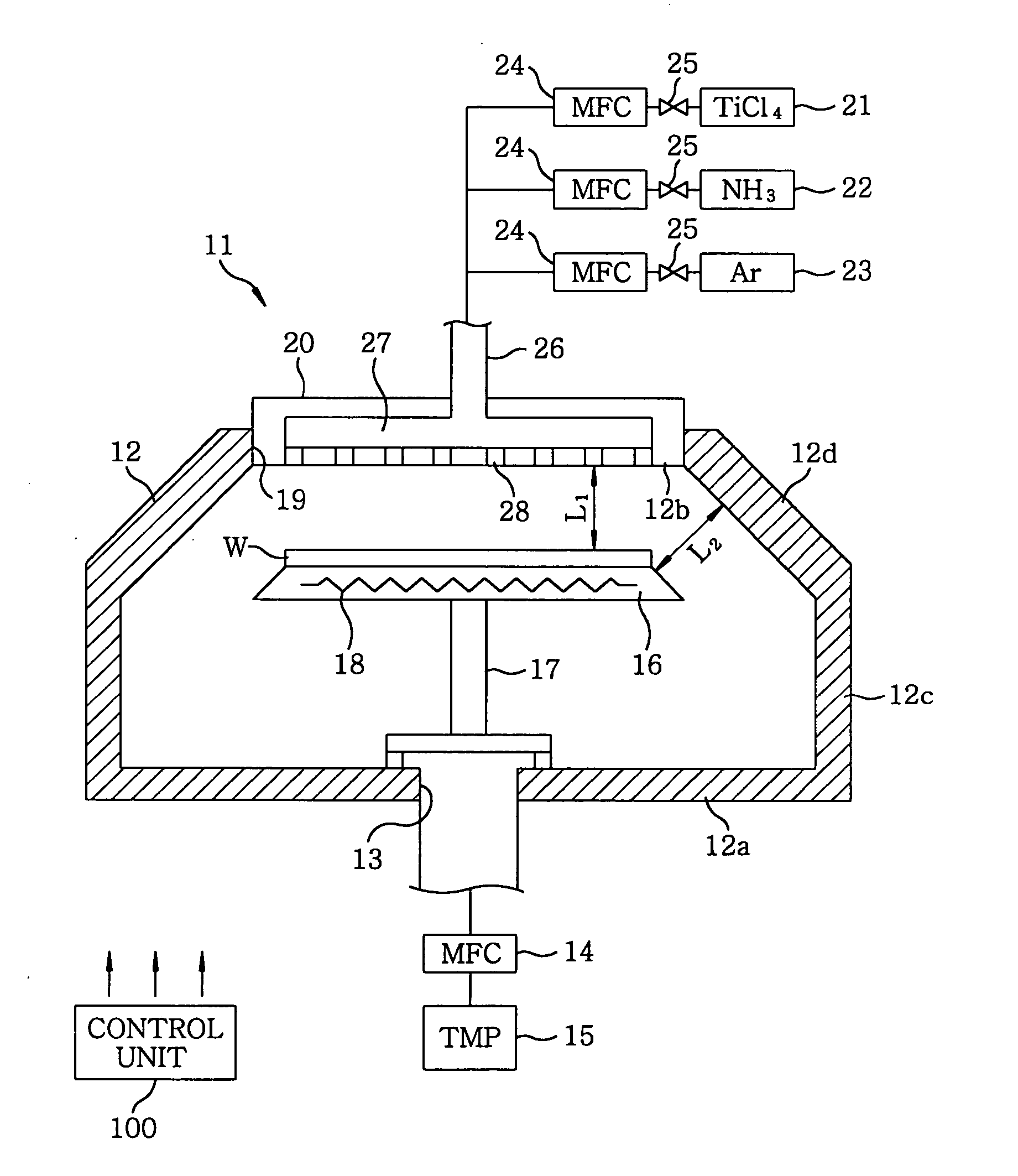
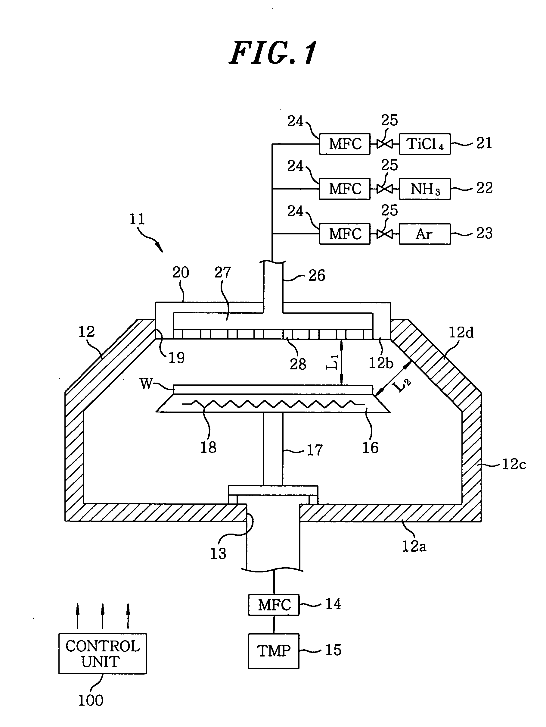
[0083] Diameter of the wafer W: 200 mm
[0084] Maximum diameter of gas supply: 200 mm
[0085] Distance L1 between the shower head 20 and the wafer W: 15 mm
[0086] Distance L2 between the side surface of the susceptor 16 and the second sidewall 12d of the chamber: 10.6 mm
[0087] Distance between the side surface of the susceptor 16 and the first sidewall 12c of the chamber: 15 mm
[0088] Inner diameter of the chamber 12 below the susceptor 16: 250 mm
PUM
| Property | Measurement | Unit |
|---|---|---|
| Time | aaaaa | aaaaa |
| Angle | aaaaa | aaaaa |
| Flow rate | aaaaa | aaaaa |
Abstract
Description
Claims
Application Information