Ionized physical vapor deposition (iPVD) process

Active Publication Date: 2005-09-29
TOKYO ELECTRON LTD
View PDF8 Cites 39 Cited by
  • Summary
  • Abstract
  • Description
  • Claims
  • Application Information

AI Technical Summary

Benefits of technology

[0006] The invention provides a method of operating an ionized physical vapor deposition (iPVD) system in which a patterned substrate is positioned on a wafer table within a processing chamber in the iPVD system; a barrier layer is deposited using a Low Net Deposition (LND) process, wherein a bias on the wafer table is adjusted

Problems solved by technology

However, as the geometries shrink and as the via dimensions go down belo

Method used


Image

  • Ionized physical vapor deposition (iPVD) process
  • Ionized physical vapor deposition (iPVD) process
  • Ionized physical vapor deposition (iPVD) process

Examples


Example

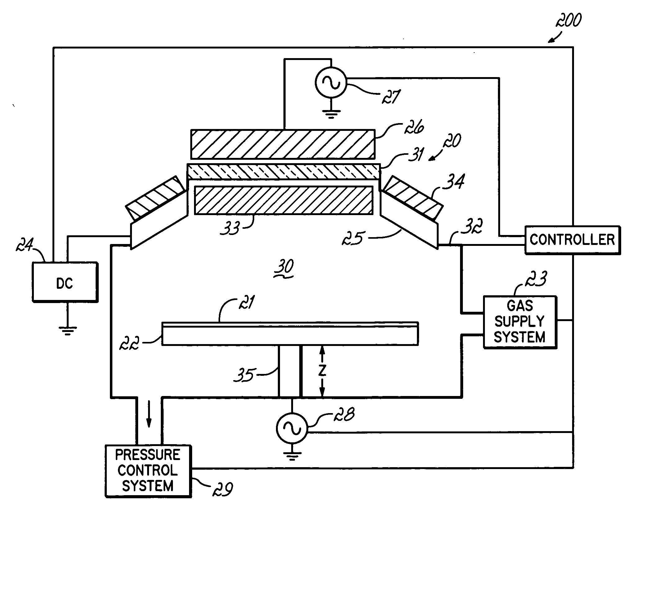
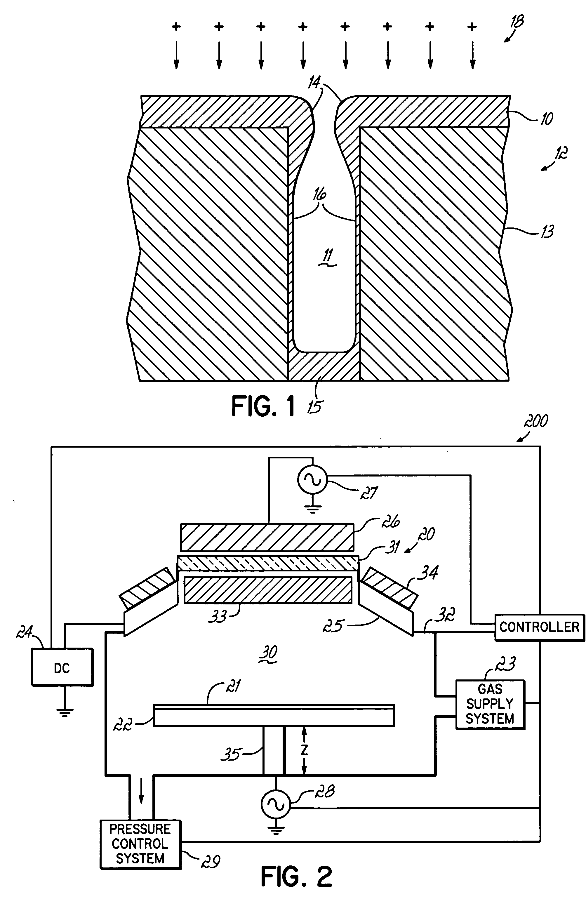
[0020] A process is described in U.S. Patent Application Publication No. 20030034244 by Yasar et al., which is copending and assigned to the assignee of the present application, that provides ionized PVD with sequential deposition and etching. While with this type of sequencing the overhang or overburden are much improved over prior processes, some will still form during the deposition sequence and may not be entirely removed in the etch sequence.

[0021] Yasar et al. describe a technique to deposit and etch multiple times within a single vacuum chamber. Overhangs are not fundamentally controlled within the deposition step of this process. Higher bias powers are typically used in the deposition step to deposit as much bottom coverage as possible before etching back the bottom to redistribute material to the sidewalls and reduce the bottom coverage, which can add to line resistance. Reduction of overhang is achieved in the subsequent etch steps.

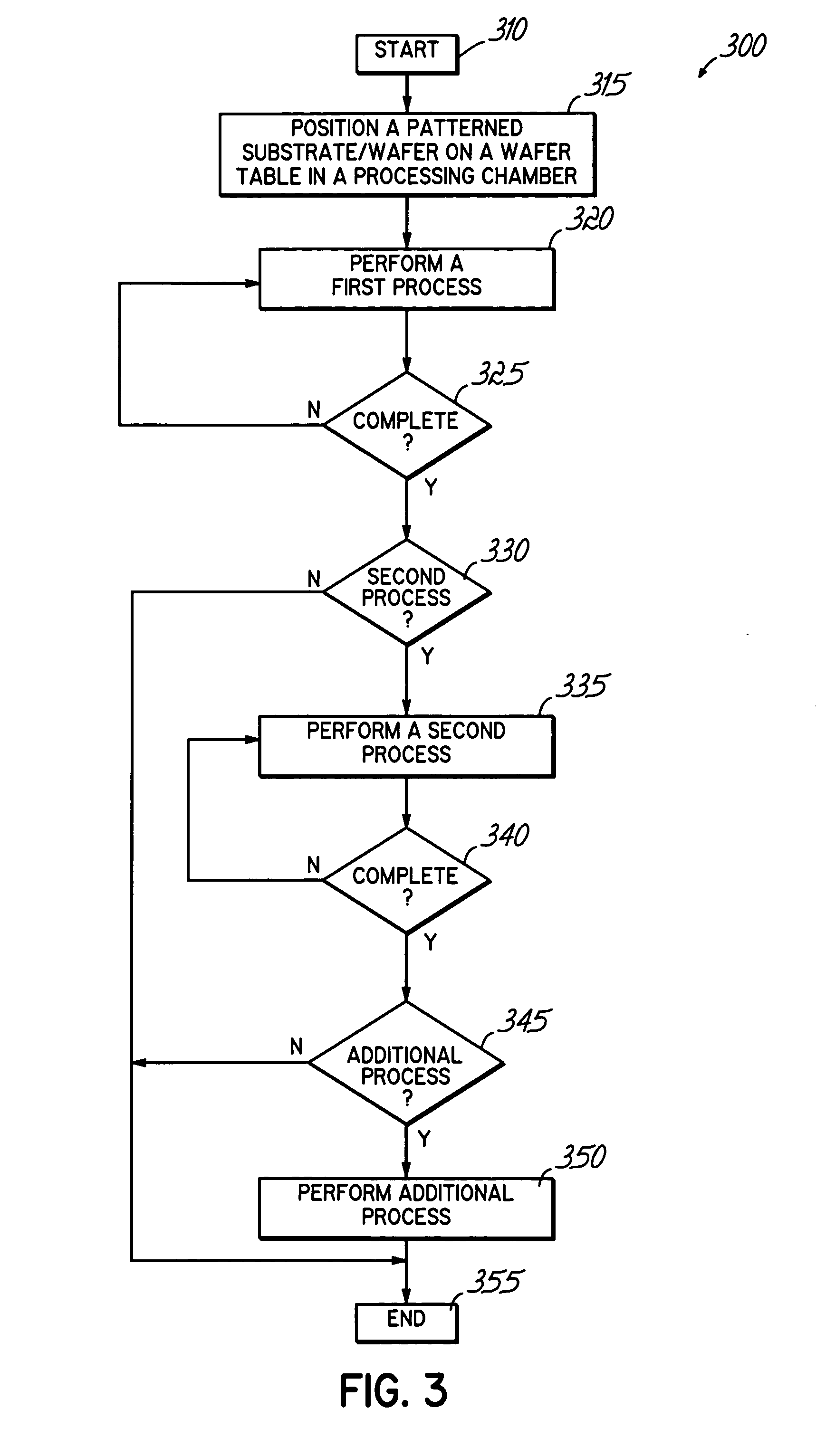
[0022] The invention provides a method ...


PUM

PropertyMeasurementUnit
Timeaaaaaaaaaa
Timeaaaaaaaaaa
Timeaaaaaaaaaa

Abstract

An iPVD system is programmed to deposit uniform material, such as barrier material, into high aspect ratio nano-size features on semiconductor substrates using a process which enhances the sidewall coverage compared to the field and bottom coverage(s) while minimizing or eliminating overhang within a vacuum chamber. The iPVD system is operated at low target power and high pressure >50 mT to sputter material from the target. RF energy is coupled into the chamber to form a high density plasma. A small RF bias (less than a few volts) can be applied to aid in enhancing the coverage, especially at the bottom.

Description

[0001] This application is related to commonly assigned and copending U.S. Patent Application Publication No. 20030034244, hereby expressly incorporated herein by reference. FIELD OF THE INVENTION [0002] The invention relates to the metallization of via and trench structures on semiconductor wafers. More particularly, the invention relates to the metallization of high aspect ratio via and trench structures of silicon wafers utilizing ionized sputtered materials to form barrier and seed layers of the substrates. BACKGROUND OF THE INVENTION [0003] In the metallization of high aspect ratio vias and trenches on semiconductor wafers, it is required that the barrier and seed layer have good sidewall coverage. [0004] Ionized PVD deposition is used for barrier and seed layer metallization in advanced IC wafers. Ionized PVD provides good sidewall and bottom coverage in via and trench structures. However, as the geometries shrink and as the via dimensions go down below 0.15 micrometers, ioniz...

Claims


Application Information

Patent Timeline
IPC IPC(8): C23C14/02C23C14/04C23C14/34H01L21/285H01L21/768
CPCC23C14/025C23C14/046C23C14/345C23C14/3492H01J37/32706H01L2221/1089H01L21/2855H01L21/76843H01L21/76865H01L21/76873H01L2221/1078H01J2237/3327C23C14/34H01L21/67207C23C14/14C23C14/02H01L21/02631
Inventor CERIO, FRANK M. JR.FAGUET, JACQUESGITTLEMAN, BRUCE D.ROBISON, RODNEY L.
Owner TOKYO ELECTRON LTD
Why Eureka
Try Eureka