Wafer, semiconductor chip, and semiconductor device manufacturing method

a semiconductor chip and manufacturing method technology, applied in semiconductor devices, semiconductor/solid-state device testing/measurement, semiconductor/solid-state device details, etc., can solve the problem that the placement information of semiconductor chips cannot be used to check for mask patterns, the number of semiconductor chips obtained cannot be increased so much, and the area occupied by scribe lines can be reduced, and the effect of facilitating error inspection of the process

Active Publication Date: 2005-09-29
RENESAS ELECTRONICS CORP
View PDF3 Cites 42 Cited by
  • Summary
  • Abstract
  • Description
  • Claims
  • Application Information

AI Technical Summary

Benefits of technology

[0010] For example, the scribe lines provided on a wafer for division into a plurality of semiconductor chips arranged in a matrix comprise, in both placement directions (the vertical direction and the horizontal direction), first-type scribe lines, of the minimum width enabling cutting using dicing, laser machining, anisotropic etching, or other means, and scribe lines of a plurality of other widths, comprising second-type scribe lines and third-type scribe lines, with line widths larger than those of first-type scribe lines so as to enable placement of TEGs comprising check transistors, alignment marks, and similar. A scribe line placement pattern is set preferably such that, within a region which can be exposed in a single shot (a unit cell), one second-type scribe line or third-type scribe line in both the vertical direction and in the horizontal direction is comprised. By this means, compared with a configuration employing only thick scribe lines, the area occupied by scribe lines can be reduced, so that the number of semiconductor chips which can be obtained from a single wafer can be increased, and consequently semiconductor chip cost reduction can be achieved.
[0011] In another aspect of the in...

Problems solved by technology

It has now been discovered that by using the above method, compared with a method of making scribe lines wider in both the vertical direction and the horizontal direction, the number of semiconductor chips obtained from a single wafer can be increased; but when the shape of semiconductor chips is nearly square, the area occupied by scribe lines in one direction (the above-described first dividing area) is increased, and the number of semiconductor chips obtained cannot be increased so much.
In structures of the above related art, the widths of scribe lines adjacent to the upper, lower, left and right edges of ea...

Method used


Image

  • Wafer, semiconductor chip, and semiconductor device manufacturing method
  • Wafer, semiconductor chip, and semiconductor device manufacturing method
  • Wafer, semiconductor chip, and semiconductor device manufacturing method

Examples


embodiment 2

[0053] Next, semiconductor devices and the manufacturing method of a second embodiment of the invention are explained, referring to FIG. 7 and FIG. 8. FIG. 7 is a plane view which schematically shows the configuration of a wafer in the second embodiment; FIG. 8 is an enlarged view of a unit cell.

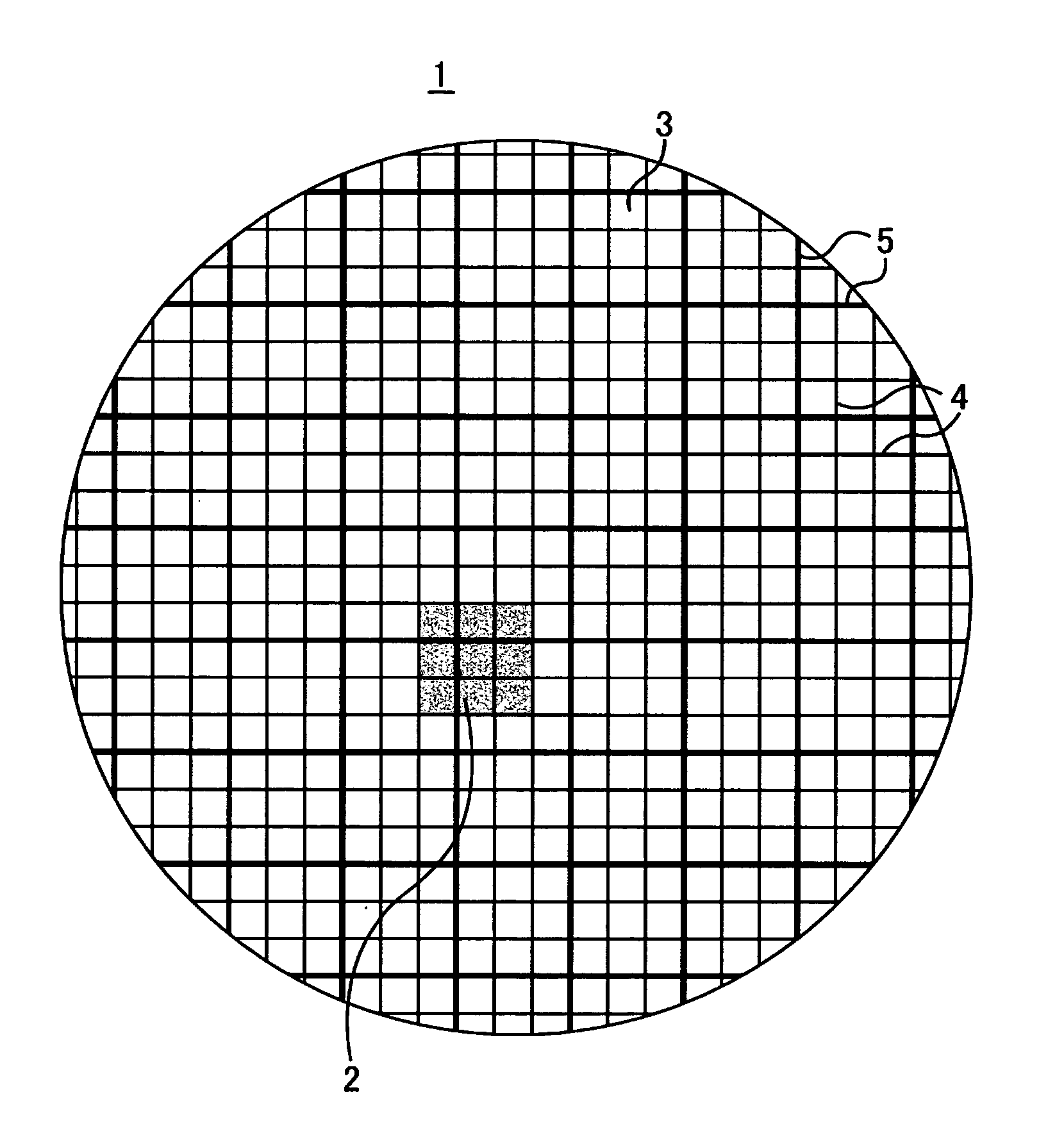
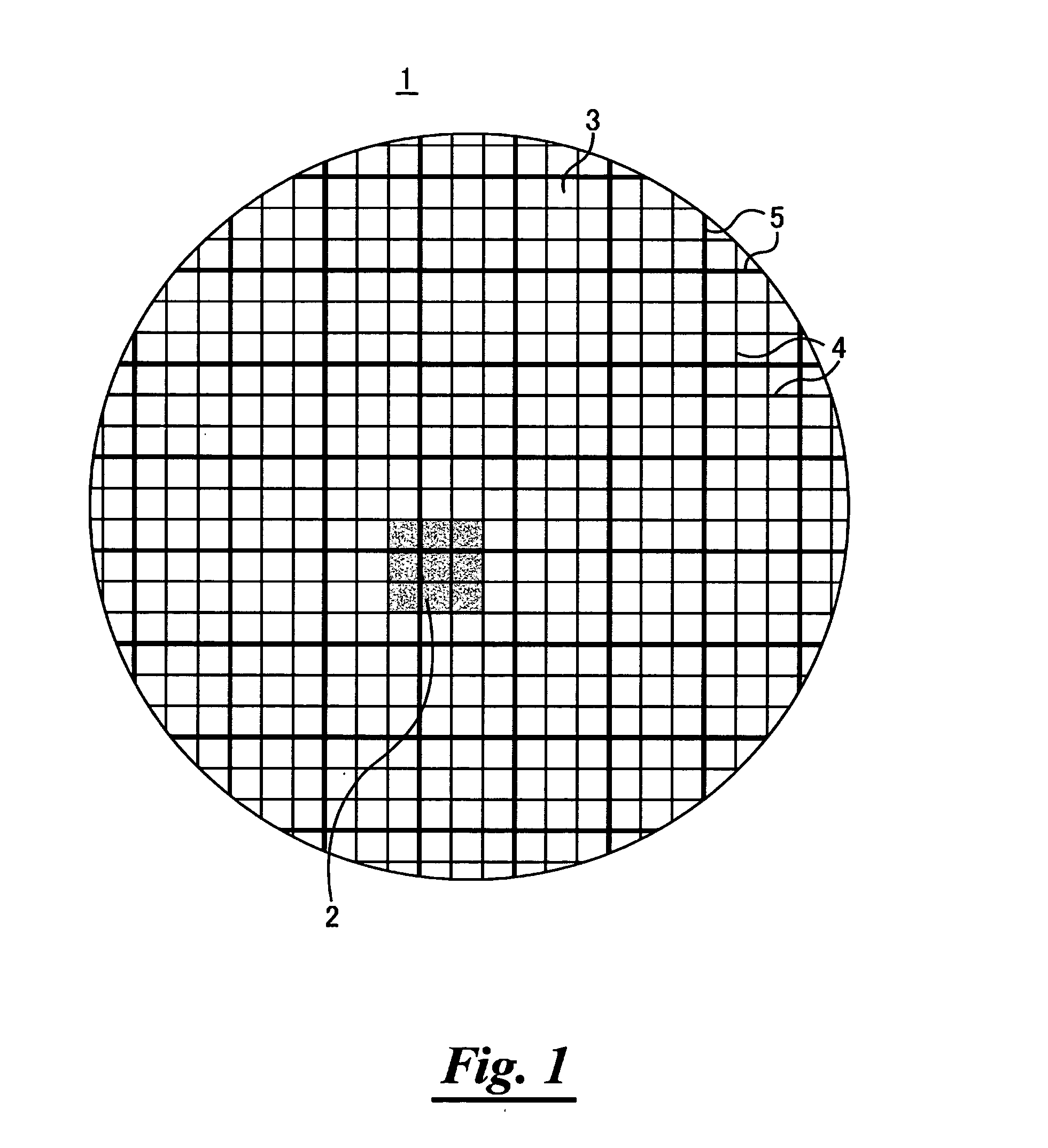
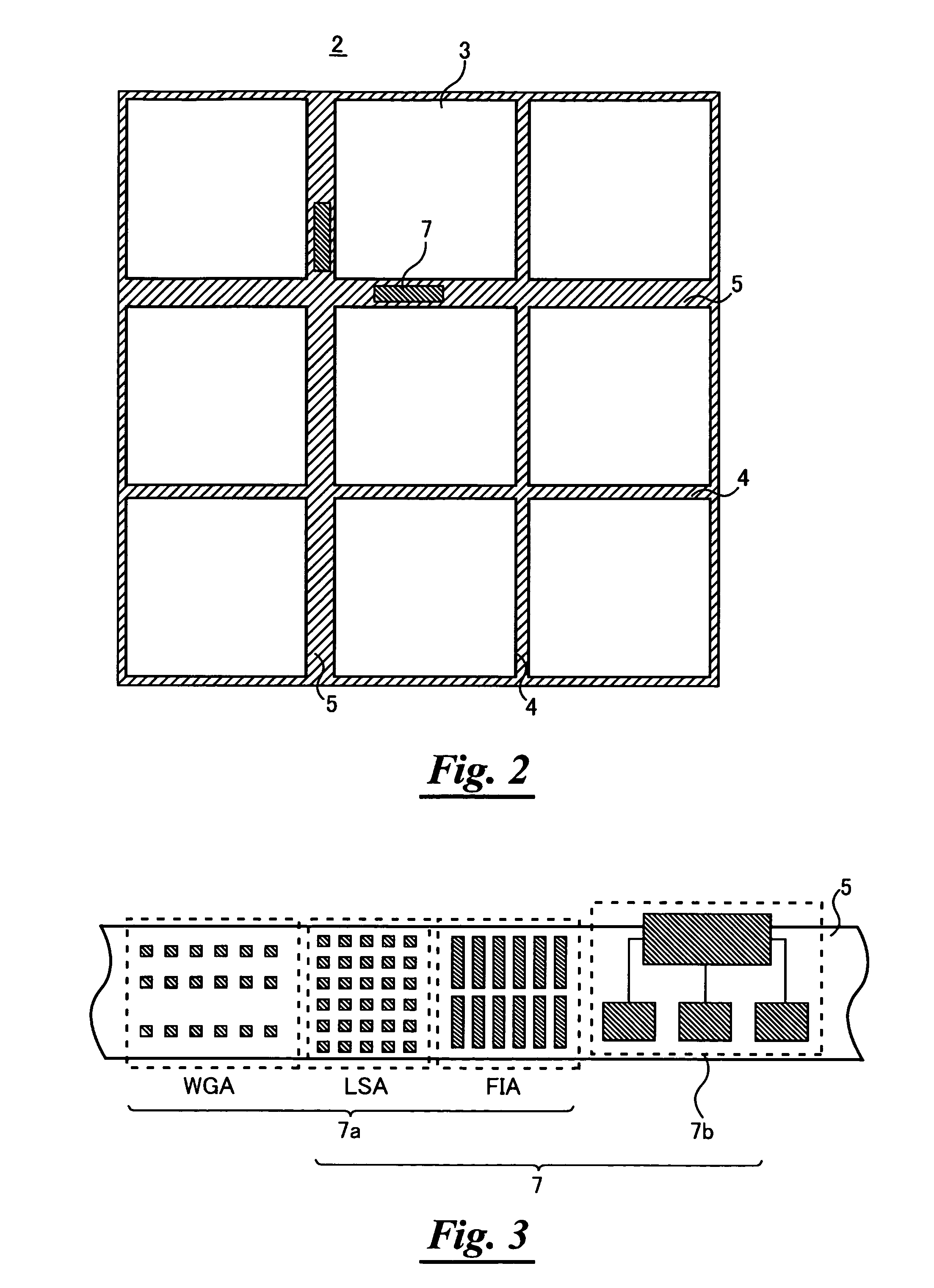
[0054] In the above-described first embodiment, there are two types of scribe lines in both the vertical direction and in the horizontal direction, which are narrow scribe with the minimum width to enable cutting, and wide scribe lines enabling placement of accessories 7, such as TEGs and alignment marks. Check transistors 7b to confirm operation of the transistors comprised within the semiconductor chips 3 must be formed with the same size and orientation as those in the semiconductor chips 3, so that when check transistors 7b have a long narrow shape, the width of the scribe lines changes according to the check transistor orientation.

[0055] In this embodiment, as shown in FIG. 7 and FIG....

embodiment 3

[0057] Next, semiconductor devices and the manufacturing method of a third embodiment of the invention are explained, referring to FIG. 9. FIG. 9 is a plane view which shows schematically the configuration of a wafer in the third embodiment.

[0058] In the above-described first and second embodiments, the semiconductor chips 3 were substantially square in shape, so that the number of semiconductor chips 3 comprising a unit cell 2 were made equal in the vertical direction and in the horizontal direction; but when semiconductor chips 3 are rectangles, if the number of semiconductor chips 3 constituting a part of a unit cell 2 is made the same in the vertical direction and in the horizontal direction, the unit cell 2 also becomes a rectangle, and as a result it may not be possible to expose the entire unit cell 2 in a single shot.

[0059] In this embodiment, rather than making the number of semiconductor chips 3 in the vertical direction and in the horizontal direction equal, the configu...


PUM


Abstract

Scribe lines demarcating semiconductor chips comprise, in both the vertical direction and the horizontal direction, first-type scribe lines of the minimum width enabling cutting by dicing or other means, and second-type scribe lines enabling placement of TEGs, alignment marks or other accessories, and a placement pattern is set so that a unit cell which can be exposed in a single shot comprises one second-type scribe line. By this means, the area occupied by scribe lines can be reduced. Further, by decreasing the number of placement of semiconductor chips constituting a unit cell, and by cutting substantially along the center line of second-type scribe lines, the shapes of scribe lines on the periphery of semiconductor chips can be changed, so that the position in the unit cell can be determined.

Description

BACKGROUND OF THE INVENTION [0001] 1. Field of the Invention [0002] This invention relates to a semiconductor chip and semiconductor device manufacturing method which facilitates defect inspection, and a wafer for obtaining such a semiconductor chip. [0003] 2. Description of the Related Art [0004] In order to achieve lower costs for semiconductor chips, it is important that the number of semiconductor chips obtained from a single wafer be increased. As shown in FIG. 10, wafers generally comprise a plurality of semiconductor chips 3 arranged in a matrix, and scribe lines 9 of a prescribed width provided between the individual semiconductor chips 3. A dicing system or similar is used to cut the wafer 1 along the scribe lines 9, to divide the wafer into individual semiconductor chips 3. [0005] A TEG (Test Element Group) comprising check transistors is formed on the wafer 1; this TEG is used to judge the quality of semiconductor chips 3 at the wafer stage. However, if a TEG is formed wi...

Claims


Application Information

Patent Timeline
IPC IPC(8): H01L21/78H01L21/301H01L23/544
CPCH01L21/78H01L22/34H01L2924/0002H01L2924/00
Inventor NISHIZAWA, KAZUYUKI
Owner RENESAS ELECTRONICS CORP
Why Eureka
Try Eureka