
Semiconductor device and manufacturing metthod thereof

a technology of semiconductor devices and semiconductor chips, applied in semiconductor devices, semiconductor/solid-state device details, electrical apparatus, etc., can solve the problems of difficult uniform and stable mounting of elastomers, inability to conduct stably bonding steps to semiconductor chips, and restricted packaging number of pins, so as to achieve low cost and improve sealing properties

Inactive Publication Date: 2005-09-29
MIYAZAKI CHUICHI +16
View PDF41 Cites 18 Cited by
  • Summary
  • Abstract
  • Description
  • Claims
  • Application Information

AI Technical Summary

Benefits of technology

"The present invention provides a semiconductor integrated circuit device with a package structure that allows for stable mounting of an elastic structural material to a wiring substrate, promoting a stable bonding step for a semiconductor chip, and enabling high-accuracy fabrication. The invention also addresses issues such as unevenness of the wiring pattern on the flexible wiring substrate, difficulty in connecting bump electrodes to the wiring substrate, and the possibility of contamination and damage to the semiconductor chip. The invention further provides a technique for simplifying the bonding process and improving the bondability, reliability, and performance of the semiconductor chip."

Problems solved by technology

For example, since the flexible wiring substrate in the package structure described above has a structure typically represented by a TCP (Tape Carrier Package) in which a Cu wiring pattern is formed on the surface of a polyimide tape, and an elastomer is formed to the wiring substrate on the side of the wiring surface, it is difficult to mount the elastomer uniformly and stably because of unevenness of the wiring pattern on the flexible wiring substrate.
That is, there exist such problems that voids not filled with the elastomer are formed near both sides of the protrusions of the wiring pattern upon coating or appending the elastomer on the flexible wiring substrate, and the step of bonding the semiconductor chip can not be conducted stably since the size and the shape of the elastomer are not stable.
Accordingly, there is a concern that an increase in the number of pins of the package may be restricted.

Method used


Image

  • Semiconductor device and manufacturing metthod thereof
  • Semiconductor device and manufacturing metthod thereof
  • Semiconductor device and manufacturing metthod thereof

Examples


embodiment 1

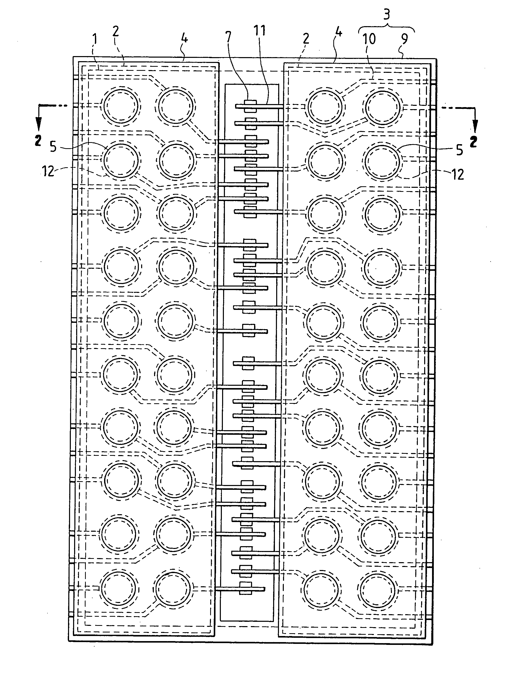
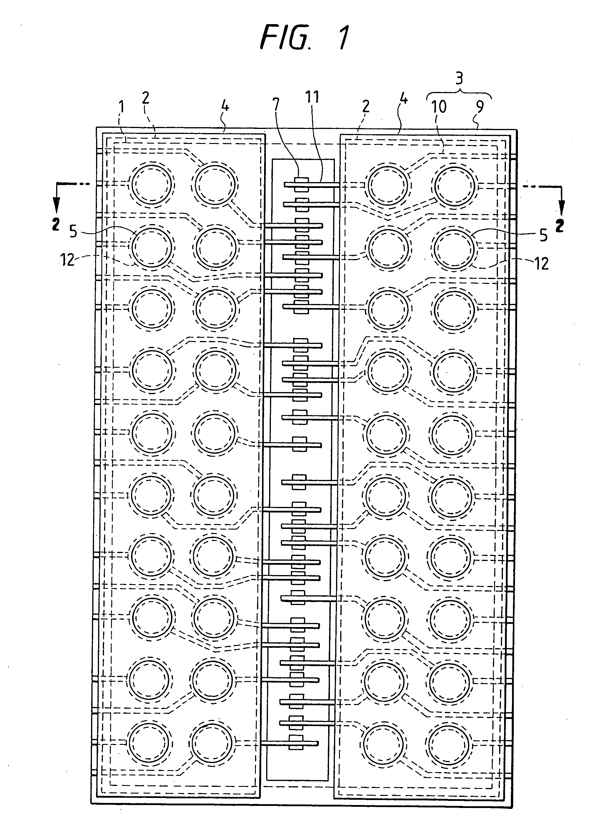
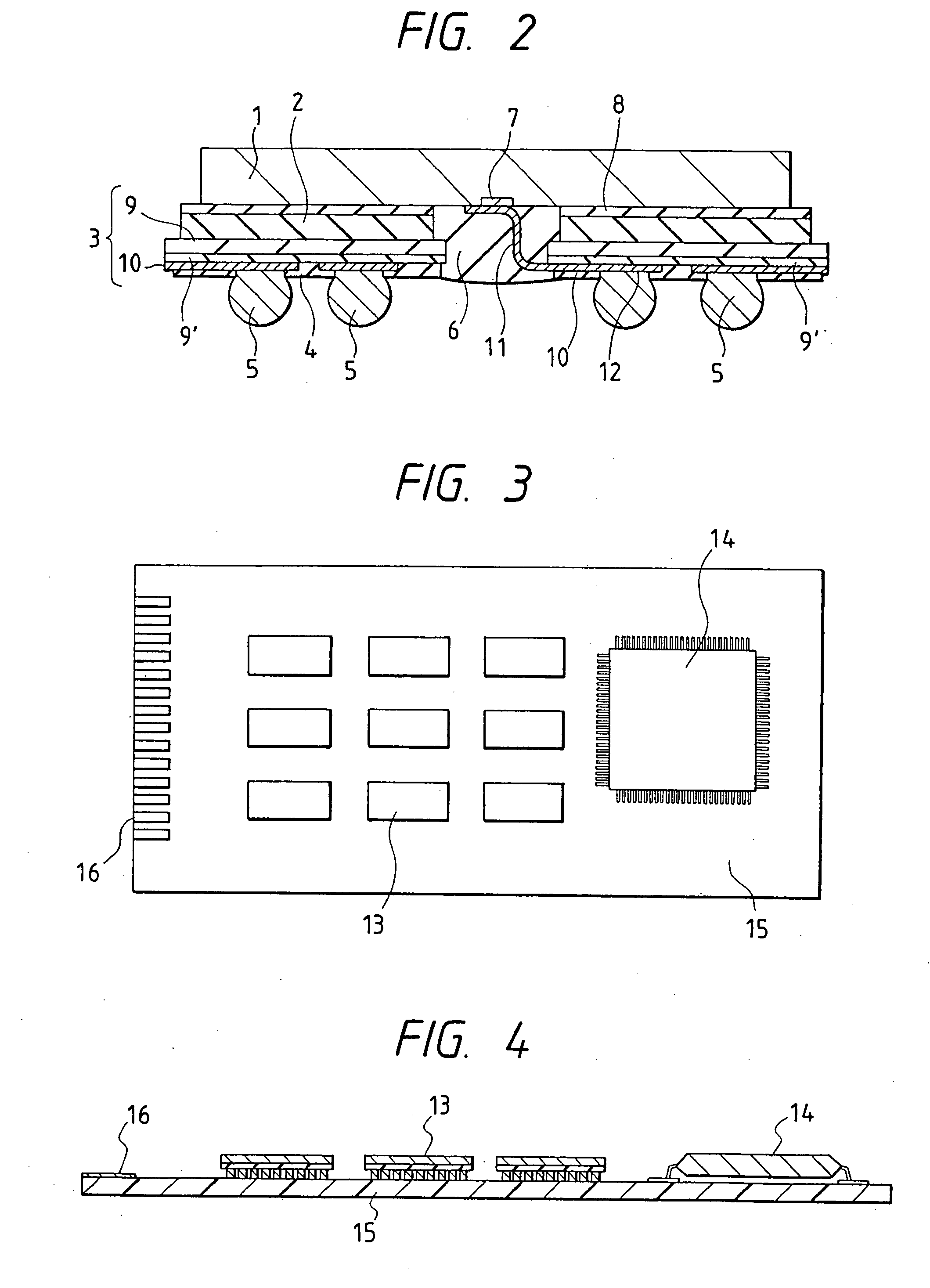
[0219]FIG. 1 is a plan view illustrating a semiconductor integrated circuit device representing an Embodiment 1 according to the present invention, FIG. 2 is a cross sectional view taken along line 2-2 in FIG. 1, FIG. 3 and FIG. 4 are a plan view and a cross sectional view illustrating a state of mounting a semiconductor integrated circuit device to a mounting substrate, FIG. 5 is a flow chart illustrating the steps (process) of assembling a semiconductor integrated circuit device, and FIG. 6 to FIG. 58 and FIG. 76 to FIG. 81 are views for comparative explanation between the feature of the semiconductor integrated circuit device representing the Embodiment 1 of the present invention and a semiconductor integrated circuit device representing a comparative example studied by the present inventors. At first, an explanation will be given as to the constitution of a semiconductor integrated circuit device of an Embodiment 1 with reference to FIG. 1 and FIG. 2.

[0220] The semiconductor in...

embodiment 2

[0355]FIG. 59 and FIG. 60 are a cross sectional view and a perspective view, respectively, illustrating a rear face wiring solder resist structure in the semiconductor integrated circuit device of Embodiment 2 according to the present invention.

[0356] The semiconductor integrated circuit device of the Embodiment 2 is a ball grid array type semiconductor package like that of the Embodiment 1, but it is different from the Embodiment 1 in that it is not based on the surface wiring technique, but is based on and provided for improving a rear face wiring structure. For instance, as shown in FIG. 59 and FIG. 60, in a structure comprising an elastomer 2 (elastic structural material) bonded on a main surface of a semiconductor chip (not shown) and a flexible wiring substrate 3 (wiring substrate) bonded to a main surface of the elastomer 2, a solder resist 56 (insulation film) is formed on the rear face of the flexible wiring substrate 3.

[0357] That is, the flexible wiring substrate 3 comp...

embodiment 3

[0365]FIG. 61 is a plan view of a semiconductor integrated circuit device forming an Embodiment 3 according to the present invention, as viewed from the rear face of a semiconductor chip, FIG. 62 is a plan view thereof, FIG. 63 is a cross sectional view thereof, FIG. 64 is an enlarged cross sectional view of a portion A in FIG. 63 and FIG. 65 is a plan view for explaining the wiring structure of the wiring substrate.

[0366] A semiconductor integrated circuit device in the Embodiment 3 adopts, instead of a semiconductor package having a structure in which the bonding pad is formed approximately at the center of the chip, as in the Embodiments 1 and 2 described above, a packaging structure using a semiconductor chip 1a in which a pad is formed to the periphery of the chip, as shown in FIG. 61 to FIG. 65, and in which bumps 5a connected to the bonding pads to the semiconductor chip 1a are disposed in a region inward of the outer circumference of the semiconductor chip 1a. The Embodimen...


PUM


Abstract

A semiconductor device includes a semiconductor chip formed with connection terminals, an elastic structure interposed between a main surface of the chip and a wiring substrate formed with wirings connected at first ends thereof to the connection terminals, and bump electrodes connected to the other ends of the wirings. The connection terminals may be at a center part or in peripheral part(s) of the chip main surface and both the elastic structure and wiring substrate are not provided at locations of connection terminals. A resin body seals at least the connection terminals and the exposed first ends of wirings (leads). In a scheme in which the connection terminals are located in a peripheral part of the chip main surface, the wiring substrate protrudes beyond the chip boundary where the connection terminals are arranged, and the resin body shape is restricted by the protruding part of the wiring substrate.

Description

[0001] This application is the first of two concurrently filed Divisional Applications of U.S. application Ser. No. 10 / 374,997, filed Feb. 28, 2003, which, in turn, is a CIP (Continuation-In-Part) of (i) U.S. application Ser. No. 09 / 768,288, filed Jan. 25, 2001, and now abandoned, of (ii) U.S. application Ser. No. 09 / 771,985, filed Jan. 30, 2001, and now abandoned, and of (iii) U.S. application Ser. No. 09 / 983,286, filed Oct. 23, 2001, and now U.S. Pat. No. 6,639,323, said U.S. application Ser. Nos. 09 / 768,288 and 09 / 771,985 are, in turn, a continuation application and a divisional application, respectively, of U.S. application Ser. No. 09 / 449,834, filed Nov. 26, 1999, and now U.S. Pat. No. 6,342,726, which, in turn, was filed as a continuation of U.S. application Ser. No. 08 / 822,933, filed Mar. 21, 1997, and now abandoned, and said U.S. application Ser. No. 09 / 983,286, is a continuation of U.S. application Ser. No. 09 / 113,500, filed Jul. 10, 1998, and now U.S. Pat. No. 6,307,269; a...

Claims


Application Information

Patent Timeline
Patent Type & Authority Applications(United States)
IPC IPC(8): H01L23/31H01L23/495H01L23/498
CPCH01L23/3114H01L23/3128H01L2224/45144H01L2924/01033H01L2924/01023H01L2924/01019H01L2924/01005H01L24/48H01L2924/3025H01L2924/15311H01L2924/1433H01L2924/14H01L2924/014H01L2924/01322H01L23/49572H01L23/49816H01L23/49827H01L23/4985H01L24/06H01L24/50H01L2224/0401H01L2224/04042H01L2224/06136H01L2224/48091H01L2224/4824H01L2224/48465H01L2224/85951H01L2924/01006H01L2924/01013H01L2924/01014H01L2924/01015H01L2924/01027H01L2924/01029H01L2924/0105H01L2924/01057H01L2924/01078H01L2924/01079H01L2924/01082H01L2924/00014H01L2924/00H01L2224/05554H01L2224/45124H01L2924/181H01L24/45H01L2224/50H01L24/86H01L2224/023H01L2924/00015H01L2224/05599H01L2924/0001
Inventor MIYAZAKI, CHUICHIAKIYAMA, YUKIHARUSHIBAMOTO, MASNORIKUDAISHI, TOMOAKIANJOH, ICHIRONISHI, KUNIHIKONISHIMURA, ASAOTANAKA, HIDEKIKIMOTO, RYOSUKETSUBOSAKI, KUNIHIROHASEBE, AKIOOHNISHI, TAKEHIROSHIMADA, NORIOUEGUCHI, SHUJIKOYAMA, HIROSHINAGAI, AKIRAOGINO, MASAHIKO
Owner MIYAZAKI CHUICHI
Learn More