Display device

a display device and display screen technology, applied in the field of image display devices, can solve the problems that devices cannot surely prevent halation, etc., and achieve the effects of excellent advantageous effect, high brightness and high contras

Inactive Publication Date: 2005-09-29
PANASONIC LIQUID CRYSTAL DISPLAY CO LTD +1
View PDF5 Cites 2 Cited by
  • Summary
  • Abstract
  • Description
  • Claims
  • Application Information

AI Technical Summary

Benefits of technology

[0024] According to the present invention, by providing a secondary electron suppressing film which prevents the reentry of the secondary electrons, which are generated when the electron beams are incident on the anode, on the back surface of the anode, even when the primary electrons impinge on the anode, the secondary electrons containing reflecting electrons are hardly emitted from the anode. Further, the trace amount of emitted secondary electrons are scattered, and these secondary electrons hardly reenter the anode due to an electric field, and, hence, halation hardly is generated in a peripheral portion of a bright display image. At the same time, the occurrence of a defocusing state in which the whole screen is blurred is reduced, whereby it is possible to achieve an excellent advantageous effect in that an image display of both high brightness and high contrast can be obtained.

Problems solved by technology

However, the display device cannot surely prevent the halation which is generated in a peripheral portion of the display image at the time of emitting light with high brightness.

Method used


Image

  • Display device
  • Display device
  • Display device

Examples


embodiment 1

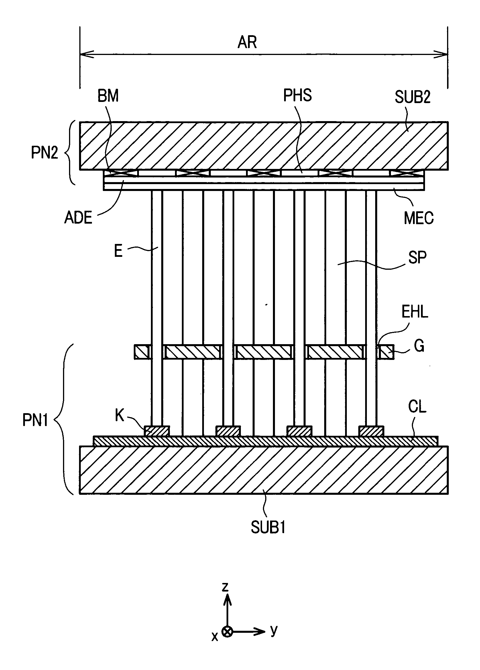
[0034]FIG. 1 is a cross-sectional view of a representative part of a FED according to one embodiment of an image display device of the present invention. In FIG. 1, symbol SUB1 indicates a back substrate which is formed of an insulation material, preferably a glass plate, and it constitutes a back panel PN1. On an inner surface of the back substrate SUB1, there are a plurality of cathode lines CL, which extend in one direction y (the vertical direction) and are arranged in parallel in another direction x (the horizontal direction), and they include cathodes K as electron sources.

[0035] Further, over the back panel PN1, control electrodes G, which cross the cathode lines CL in a non-contact state, extend in the x direction and are arranged in parallel in the y direction, and they are arranged to face the back panel PN1 in a non-contact state. Here, the control electrodes G form pixels at crossing portions of the control electrodes G and the cathode lines CL, and a plurality of elect...

embodiment 2

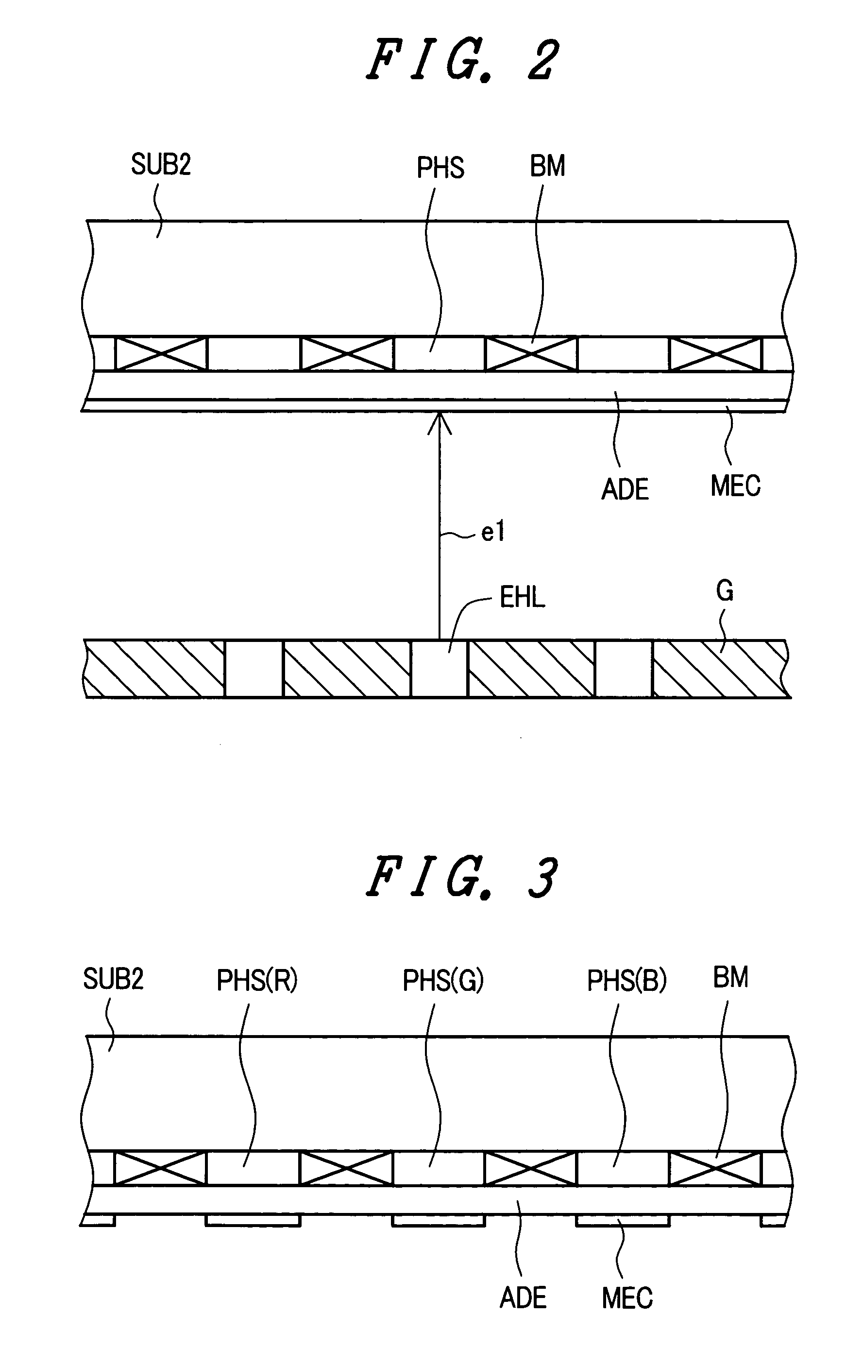
[0045]FIG. 4 is an enlarged cross-sectional view of an FED representing another embodiment of the image display device according to the present invention. In the FED shown in FIG. 4, as well as in FIG. 1, between the face substrate SUB2 and the back substrate SUB1, distance holding members SP, which maintain a given distance between the face substrate SUB2 and the back substrate SUB1, are provided. These distance holding members SP are formed of a thin plate made of glass or ceramics, for example, and they are arranged in an erect manner at positions which avoid the pixels, for example, on the black matrix BM.

[0046] In this embodiment, as shown in FIG. 4, the carbon film MEC, which constitutes a secondary electron suppressing film formed on the back surface of the anode ADE, is formed in regions which avoid the distance holding members SP. Also, in this case, the carbon film MEC can be easily formed by a method in which fine carbon powder is dispersed in a binder, and the mixture i...


PUM


Abstract

The present invention provides an image display device in which it is possible to obtain an image display of high brightness and high contrast by preventing the halation which may be generated in a peripheral portion of a display image. By providing a carbon film which attenuates the reentry of secondary electrons, which are generated when electron beams impinge on an anode, to a back surface of the anode, even when primary electrons impinge on the anode, the secondary electrons are hardly emitted from the anode. At the same time, a trace amount of emitted secondary electrons are mainly formed of electrons having a small energy. Hence, these emitted secondary electrons are scattered and hardly reenter the anode.

Description

BACKGROUND OF THE INVENTION [0001] The present invention relates in general to an image display device of the type which utilizes the emission of electrons in a vacuum which is created between a face substrate and a back substrate; and, more particularly, the invention relates to a secondary electron emission suppression structure which can reduce the reentry of secondary electrons that are generated when electron beams impinge on an anode. [0002] As a display device which exhibits high brightness and high definition, color cathode ray tubes have been widely used conventionally. However, along with the recent demand for images of higher quality in information processing equipment or television broadcasting, the demand for planar displays (panel displays), which are light in weight and require a small space, while exhibiting high brightness and high definition, has been increasing. [0003] As typical examples, liquid crystal display devices, plasma display devices and the like have be...

Claims


Application Information

Patent Timeline
Patent Type & Authority Applications(United States)
IPC IPC(8): F16F15/02G05B13/04B60K5/12G05D19/02G09F9/00G10K11/16G10K11/178H01J29/18H01J29/28H01J31/12H01J31/15
CPCG05B13/042H01J31/15H01J29/467H01J29/18H01J2329/323
Inventor HIRASAWA, SHIGEMIKIJIMA, YUUICHIKAWASAKI, HIROSHI
Owner PANASONIC LIQUID CRYSTAL DISPLAY CO LTD
Why Eureka
Try Eureka