Method and apparatus for package testing

a technology of package design and test method, applied in the direction of electronic circuit testing, measurement device, instruments, etc., can solve the problems of high undesirable failure of integrated circuit, inability to accept incompatibility between package and die, and high cost of package design, so as to reduce the cost and time to market of functional devices

Inactive Publication Date: 2005-09-29
MINDSPEED TECH INC
View PDF1 Cites 9 Cited by
  • Summary
  • Abstract
  • Description
  • Claims
  • Application Information

AI Technical Summary

Benefits of technology

[0018] In one variation of this embodiment, the method further comprises, responsive to the comparing, determining if the package passed the package testing procedure. To reduce costs and time to market of a functional device, the test die comprises a non-functional die configured for package testing. In addition, the bias signal may be applied to the test device to thereby establish opposing electrical polarities on one or more conductors within the package, on the test die, or both. In one embodiment, the test die comprises two or more layers of metal and insulator.
[0019] A package test device is

Problems solved by technology

In addition, certain applications for electronic circuits require that the package protect the die in extreme and harsh conditions.
As is understood by those of ordinary skill in the art, package design is a complex and time-consuming process.
As can be appreciated, it is highly undesirable for an integrated circuit to fail after a few months of service due to a failure of the package to adequately protect and secure the integrated circuit.
Likewise, it is not acceptable for there to be some incompatibility between the package and the die.
HAST procedures subject the functional device to a highly abusive environment for a period of time.
While this prior art method of package design and material set validation adequately tested the package, it suffers from numerous drawbacks.
One such drawback is that the prior art procedure for testing utilizes a functional device and thus, it occurs at the end of the functional die design cycle, i.e. after a package containing a die has undergone functional testing.
However, performing the HAST at the end after the device is functional, results in flaws or failure in the package design or material set becoming known just prior to anticipated product launch.
As can be appreciated, this is a highly undesirab

Method used


Image

  • Method and apparatus for package testing
  • Method and apparatus for package testing
  • Method and apparatus for package testing

Examples


Embodiment Construction

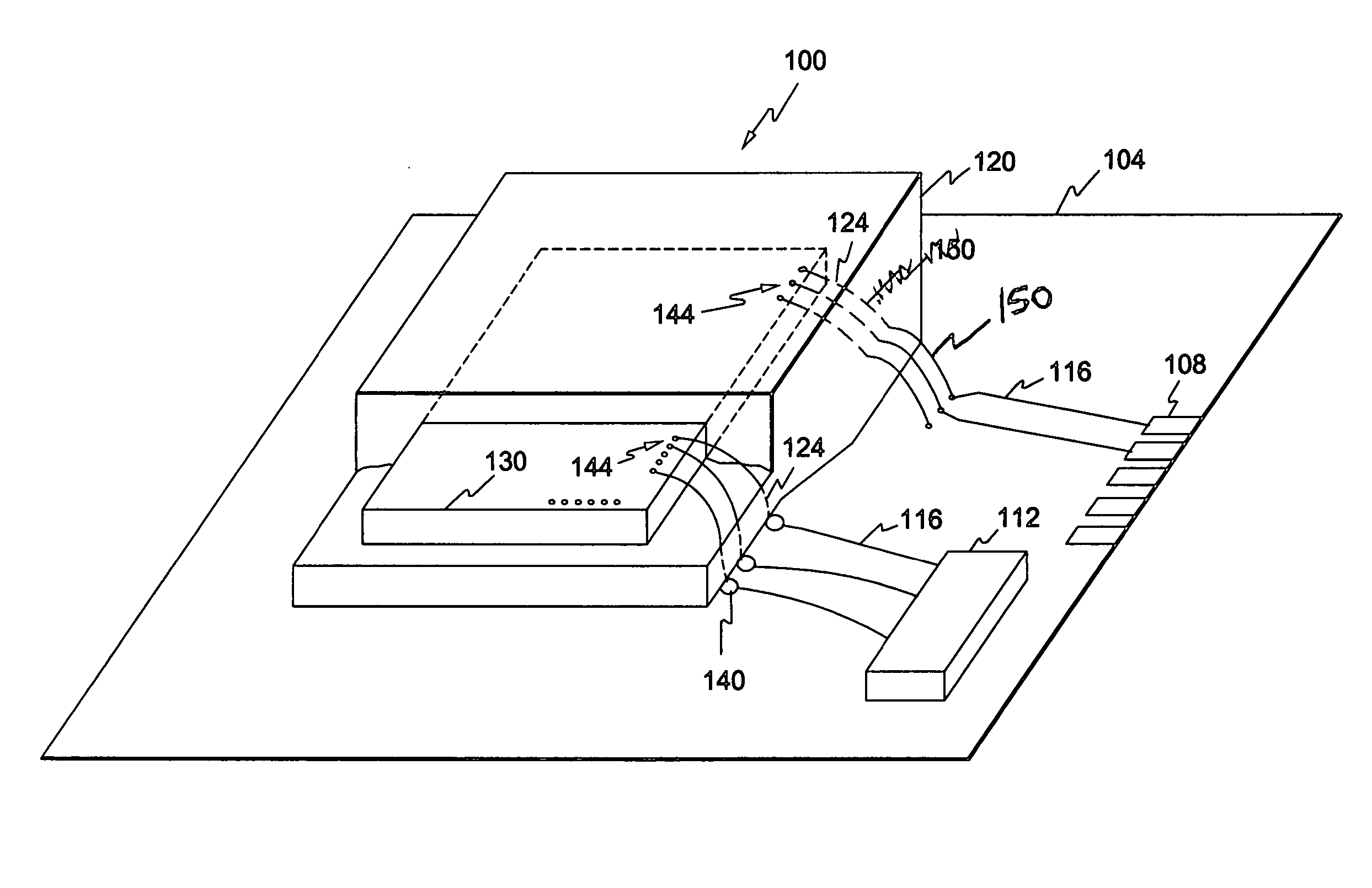
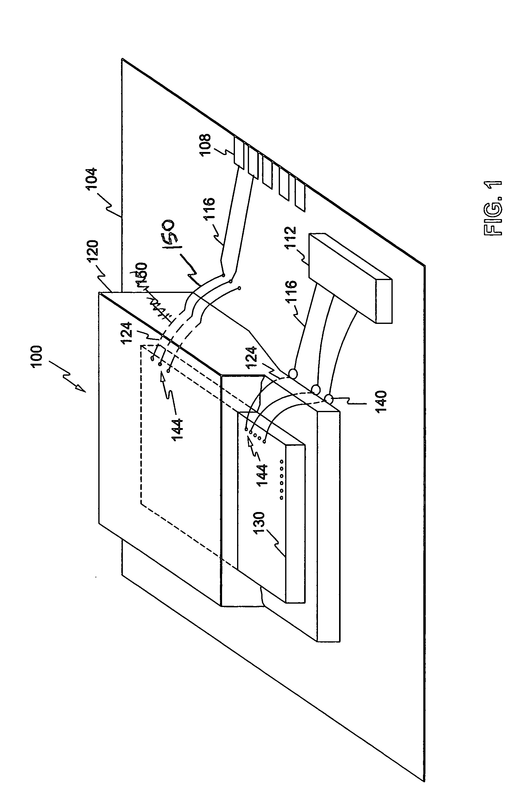
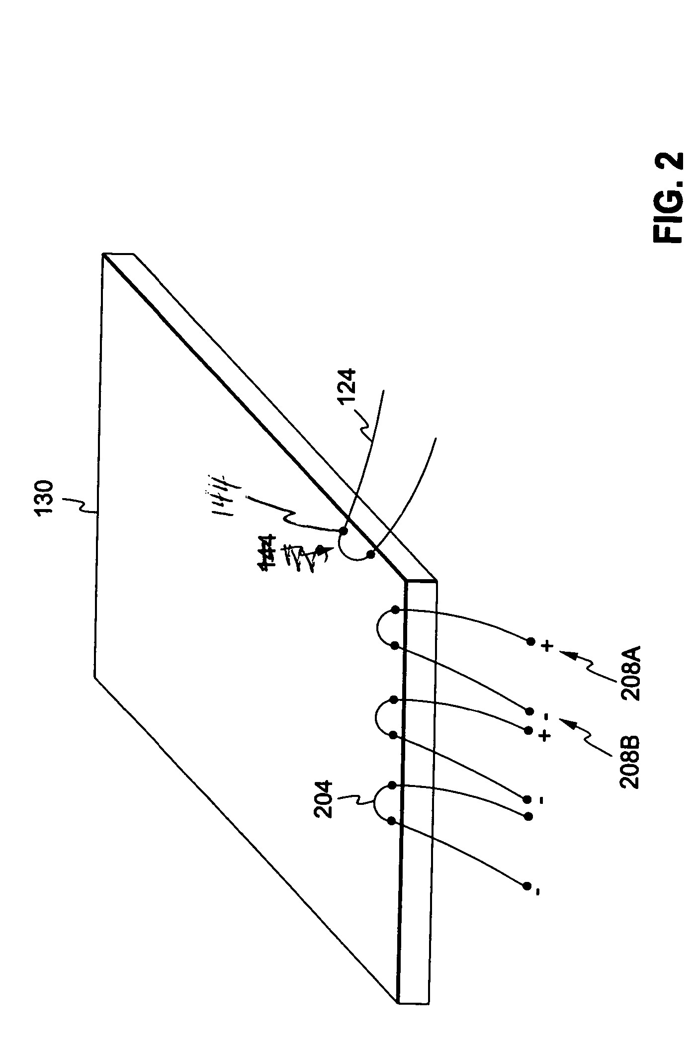
[0031]FIG. 1 illustrates a perspective cut away view of an example embodiment of a test device 100 mounted on a circuit board 104. The circuit board 104 may comprise any type surface or structure configured to electrically connect a test die 130 and package 120 to one or more contacts 108 or connectors 112. In this embodiment the board 104 is configured with one or more contacts 108 or one or more connectors 112 configured to allow for electrical connection to the package 120. The contacts 108 or connectors 112 may comprise any type contact or connector capable of conveying an electrical signal or bias to the test device 100. Although it is contemplated that the board 104 may have both board contacts 108 and connectors 112, in many embodiments the board will have only one or the other for providing bias or test signals to the test device 100. One or more conductive circuit board traces 116 electrically connect the contacts 108 or connectors 112 to the test device 100.

[0032] The tes...


PUM


Abstract

A method and apparatus for testing a package design and material set comprising using a test die to form a test device and subjecting the test device to a test procedure, such as a highly accelerated stress test (HAST). In one embodiment the device, which comprises a die and a package to be tested, is constructed using a test die. The test die comprises a non-functional die having one or more conductive traces thereon. Use of a test die reduces costs as compared to a functional die and reduces the time to market by allowing package testing prior to creation and testing of a functional die. In one embodiment the test die is configure with conductive traces on its top surface to allow for biasing before, during, or after testing.

Description

FIELD OF THE INVENTION [0001] The invention relates to semiconductor design and manufacture and in particular to a method and apparatus for performing a package testing using a test die. RELATED ART [0002] There exists a continuing demand for the electronic devices that have greater functionality and speed than was previously available. As such, there have been and continue to be great strides in the development of new integrated circuit technologies. By way of example, electronic circuits increasingly operate at higher speeds and enjoy reductions in size. [0003] By way of background, an electronic “chip” is often referred to generally as a single component, but it actually comprises numerous subparts. As is generally understood, the “chip” comprises a die or integrated circuit configured with one or more circuits. In particular, the die comprises one or more metallic layers, insulating layers, and one or more ion implanted regions. The die is housed within a package that protects a...

Claims


Application Information

Patent Timeline
IPC IPC(8): G01R31/02G01R31/26G01R31/28
CPCG01R31/2896
Inventor LYNCH, MARK
Owner MINDSPEED TECH INC
Why Eureka
Try Eureka