Transflective liquid crystal device and electronic apparatus using the same

a liquid crystal device and electronic equipment technology, applied in non-linear optics, instruments, optics, etc., can solve the problems of unevenness on the surface of the substrate, retardation (nd) cannot be held in enhanced or optimal state, etc., to achieve wide chromaticity region and wide chromaticity region

Inactive Publication Date: 2005-09-29
BOE TECH GRP CO LTD
View PDF9 Cites 8 Cited by
  • Summary
  • Abstract
  • Description
  • Claims
  • Application Information

AI Technical Summary

Benefits of technology

[0029] In the present invention, the color filter for transmission display preferably has a wide chromaticity region, for example, due to different kinds of color materials or blending amount from those of the color filter for reflection display. That is, if layer thickness of the color filter for transmission display is made to be thicker than that of the color filter for reflection display to widen the chromaticity region, the effect by the layer-thickness adjusting layer can be damaged. However, if the chromaticity region of the color filter for transmission display is made to be wider than that of the color filter for reflection display due to different kinds of color materials or blending amount, the damage of the effect by the layer-thickness adjusting layer does not occur. On the contrary, layer thickness of the color filter for reflection display can be made to be thicker than that of the color filter for transmission display, and therefore, the layer thickness balance of the liquid crystal layer between the transmission display region and the reflection display region can be enhanced or optimized by the layer thickness difference of the color filters.

Problems solved by technology

However, if the retardation (Δn·d) is enhanced or optimized by forming the layer-thickness adjusting layer, an unevenness is formed on the surface of the substrate due to the layer-thickness adjusting layer.
As a result, even though trying to control the TFT array substrate 10 and the counter substrate 20 by dispersing a gap material 5 on the surface of the counter substrate 20, or when assembling a liquid crystal device, the gap material comes into a concave portion generated due to the layer-thickness adjusting layer so that the non-uniformity of the substrate gap occurs during the process of manufacturing a liquid crystal device or after the liquid crystal device is manufactured, which results in a problem in which the retardation (Δn·d) cannot be held in an enhanced or optimum state.

Method used


Image

  • Transflective liquid crystal device and electronic apparatus using the same
  • Transflective liquid crystal device and electronic apparatus using the same
  • Transflective liquid crystal device and electronic apparatus using the same

Examples


first exemplary embodiment

(Basic Structure of a Transflective Liquid Crystal Device)

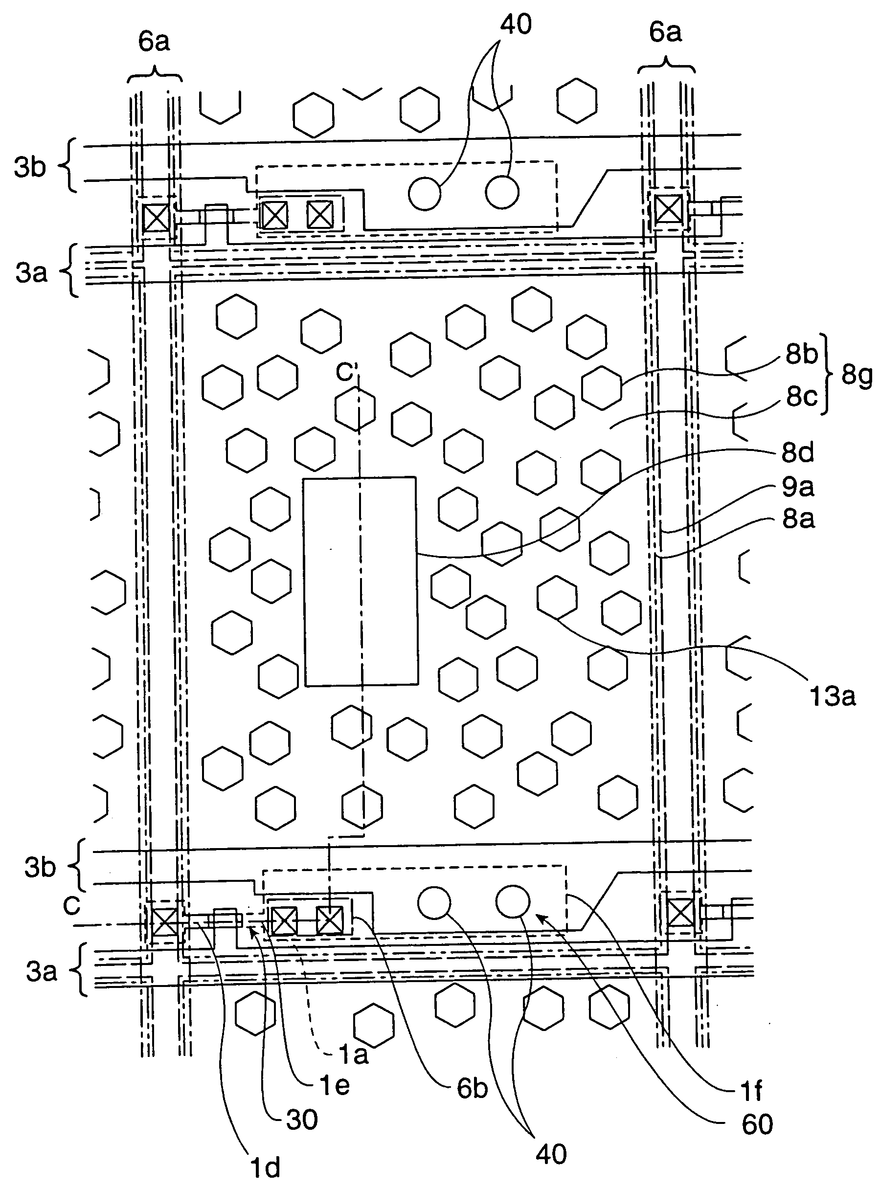
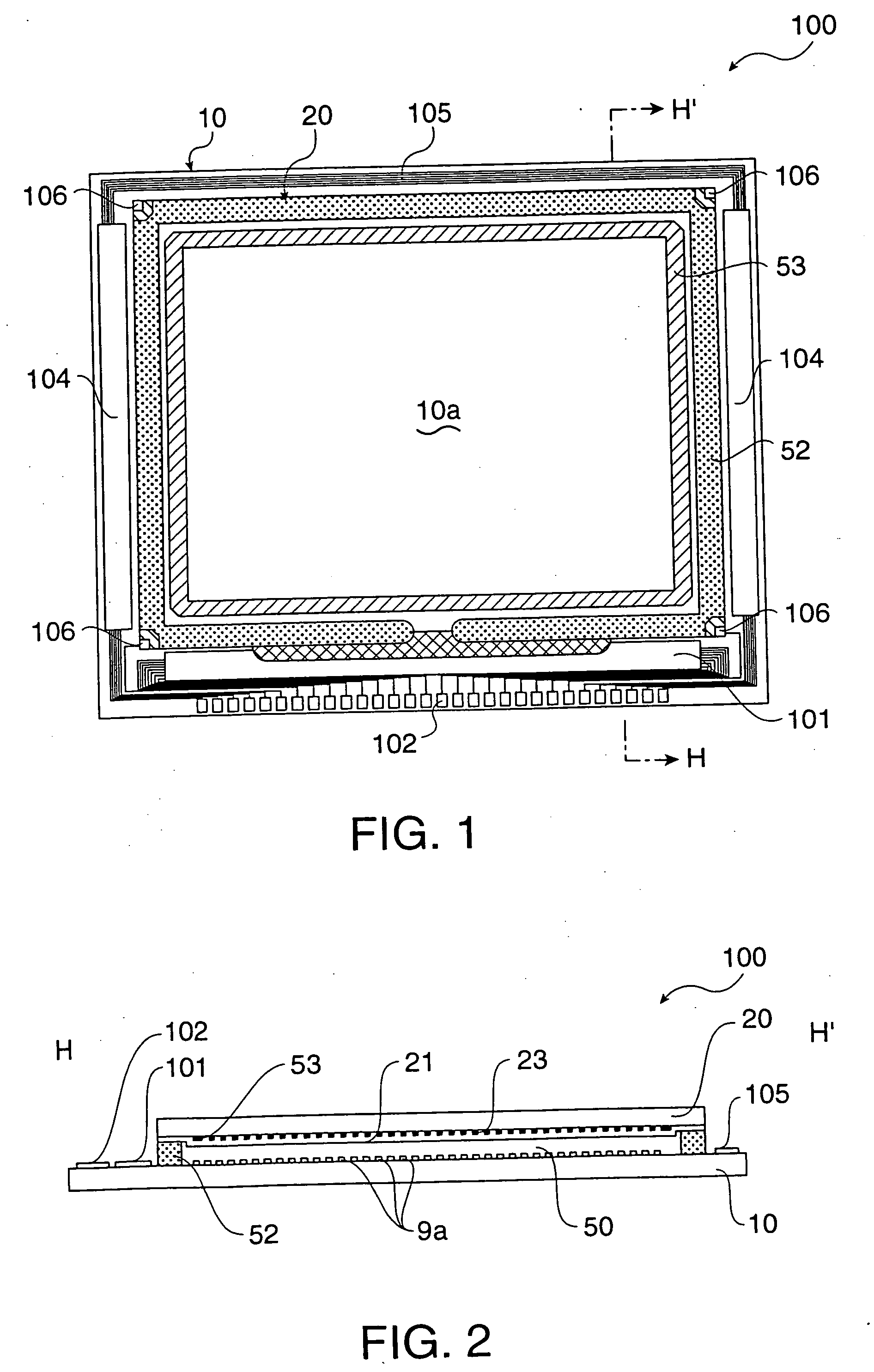
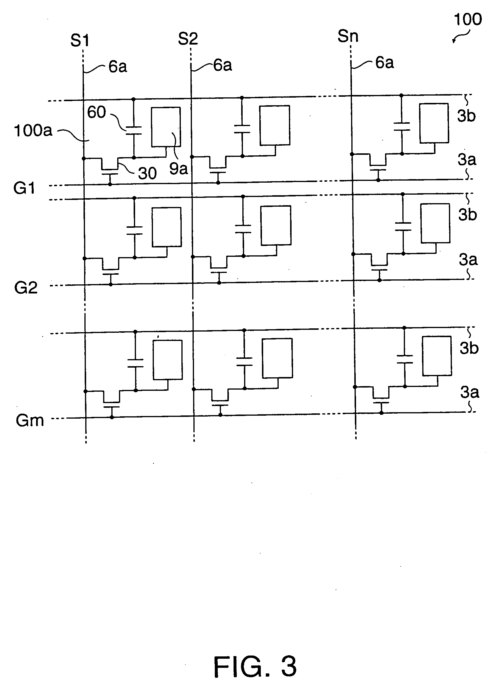
[0056]FIG. 1 is a plan view of a transflective liquid crystal device according to the present invention as viewed at component elements and a counter substrate, and FIG. 2 is a sectional view taken along plane H-H′ of FIG. 1. FIG. 3 is a schematic circuit diagram showing various elements, wirings, etc. in a plurality of pixels formed in a matrix shape in the image display region of the transflective liquid crystal device. Further, in the following description, the scales of layers or members in each of the drawings are different since each layer or member is merely drawn with a size to be recognizable in the drawings.

[0057] As shown in FIGS. 1 and 2, a transflective liquid crystal device 100 of the present invention is configured such that a liquid crystal layer 50 as an electric optical material is held between a TFT array substrate 10 (a first transparent substrate) and a counter substrate 20 (a second transparent substr...

second exemplary embodiment

[0083]FIG. 6 is a sectional view of a part of the pixel of the transflective liquid crystal device according to a second exemplary embodiment of the present invention taken along plane C-C′ of FIG. 4. Further, in the configuration of this exemplary embodiment and any configuration to be described below, a basic structure is the same as that of the first exemplary embodiment. Therefore, the common elements are designated with the same numerals to omit the description thereof, and only the structure of a counter substrate which is a feature of each exemplary embodiment are explained.

[0084] On a counter substrate 20 shown in FIG. 6, the layer thickness “d” of a liquid crystal layer 50 in a reflection display region 100b is considerably thinner than the layer thickness “d” of a liquid crystal layer 50 in a transmission display region 100c by a transparent layer-thickness adjusting layer 25 selectively formed in the reflection display region 100b. Due to such a structure, the retardatio...

third exemplary embodiment

[0091]FIG. 8 is a sectional view of a part of the pixel of the transflective liquid crystal device according to a third exemplary embodiment of the present invention taken along plane C-C′ of FIG. 4.

[0092] In the first and second exemplary embodiments, the layer-thickness adjusting layer 25 is formed between the counter electrode 21 and the color filter. However, in this exemplary embodiment, as shown in FIG. 8, a transparent layer-thickness adjusting layer 25 is selectively formed in a reflection display region 100b below a color filter for transmission display 241 formed in a transmission display region 100c, and a color filter for reflection display 242 formed in a reflection display region 100b.

[0093] Due to such a structure, the layer thickness “d” of a liquid crystal layer 50 in a reflection display region 100b is considerably thinner than the layer thickness “d” of a liquid crystal layer 50 in a transmission display region 100c. Therefore, the retardation (Δn·d) can be enha...


PUM

PropertyMeasurementUnit
thicknessaaaaaaaaaa
thicknessaaaaaaaaaa
thicknessaaaaaaaaaa

Abstract

The invention provides a transflective liquid crystal device and an electronic apparatus using the same which do not cause a non-uniformity in the substrate gap, even though a layer-thickness adjusting layer is formed so that the layer thickness balance of a liquid crystal layer between a transmission display region and a reflection display region is optimized thereby. Below a counter electrode of a counter substrate of a transflective liquid crystal device, a color filter for transmission display, being thin and having a wide chromaticity region, is formed in a transmission display region, and a color filter for reflection display, being thick and having a narrow chromaticity region, is formed in a reflection display region. Further, the interval between a TFT array substrate and the counter substrate is adjusted by a columnar protrusion formed on the TFT array substrate, and a gap material is not dispersed between the TFT array substrate and the counter substrate.

Description

CROSS-REFERENCE TO RELATED APPLICATION [0001] This is a Division of application Ser. No. 10 / 440,274 filed May 19, 2003. The entire disclosure of the prior application is hereby incorporated by reference herein in its entirety.BACKGROUND OF THE INVENTION [0002] 1. Field of Invention [0003] The present invention relates to a transflective liquid crystal device having a reflection display region and a transmission display region in one pixel. The invention also relates to electronic apparatuses including the same. [0004] 2. Description of Related Art [0005] Related art liquid crystal devices that are capable of displaying images in both a transmission mode and a reflection mode are referred to as transflective liquid crystal devices, and can be used in many applications. [0006] In such a transflective liquid crystal device, as shown in FIG. 21, an active matrix-type transflective liquid crystal device includes a TFT array substrate 10 (first transparent substrate) having a transparent ...

Claims


Application Information

Patent Timeline
Patent Type & Authority Applications(United States)
IPC IPC(8): G02F1/1335G02F1/1333G02F1/1339G02F1/1343
CPCG02F2203/09G02F1/13394G02F1/1335
Inventor MURAI, ICHIROITOH, TOMOYUKI
Owner BOE TECH GRP CO LTD
Why Eureka
Try Eureka