Large scale patterned growth of aligned one-dimensional nanostructures

a nanostructure and one-dimensional technology, applied in the field of nanostructures, can solve the problems of uncontrollable properties, difficult control of the structure and morphology of many nanostructures, and difficult investigation of wire-like semiconducting oxide nanostructures

Active Publication Date: 2005-10-13
GEORGIA TECH RES CORP
View PDF6 Cites 94 Cited by
  • Summary
  • Abstract
  • Description
  • Claims
  • Application Information

AI Technical Summary

Benefits of technology

[0020] In another aspect, the invention is a field effect transistor circuit that includes a first nano-bowl structure and a second nano-bowl structure in vertical alignment with the first-nanobowl structure. The first nano-bowl structure includes a conductive substrate, an insulating layer disposed on the conductive substrate, a nano-bowl disposed on the insulating layer and an elongated nanostructure extending from the conductive substrate through the insulating layer into the nano-bowl and electrically isolated from the nano-bowl. Similarly, the second nano-bowl structure includes a conductive substrate, an insulating layer disposed on the conductive substrate, a nano-bowl disposed on the insulating layer and an elo...

Problems solved by technology

In contrast, investigations of wire-like semiconducting oxide nano structures can be difficult due to the unavailability of nanowire structures.
However, the nanostructures discussed above can have a variety of deficiencies.
For example, often it is difficult to control the structure and morphology of many nanostru...

Method used


Image

  • Large scale patterned growth of aligned one-dimensional nanostructures
  • Large scale patterned growth of aligned one-dimensional nanostructures
  • Large scale patterned growth of aligned one-dimensional nanostructures

Examples


Embodiment Construction

[0036] A preferred embodiment of the invention is now described in detail. Referring to the drawings, like numbers indicate like parts throughout the views. As used in the description herein and throughout the claims, the following terms take the meanings explicitly associated herein, unless the context clearly dictates otherwise: the meaning of “a,”“an,” and “the” includes plural reference, the meaning of “in” includes “in” and “on.”

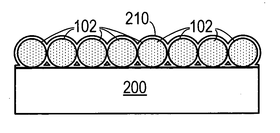
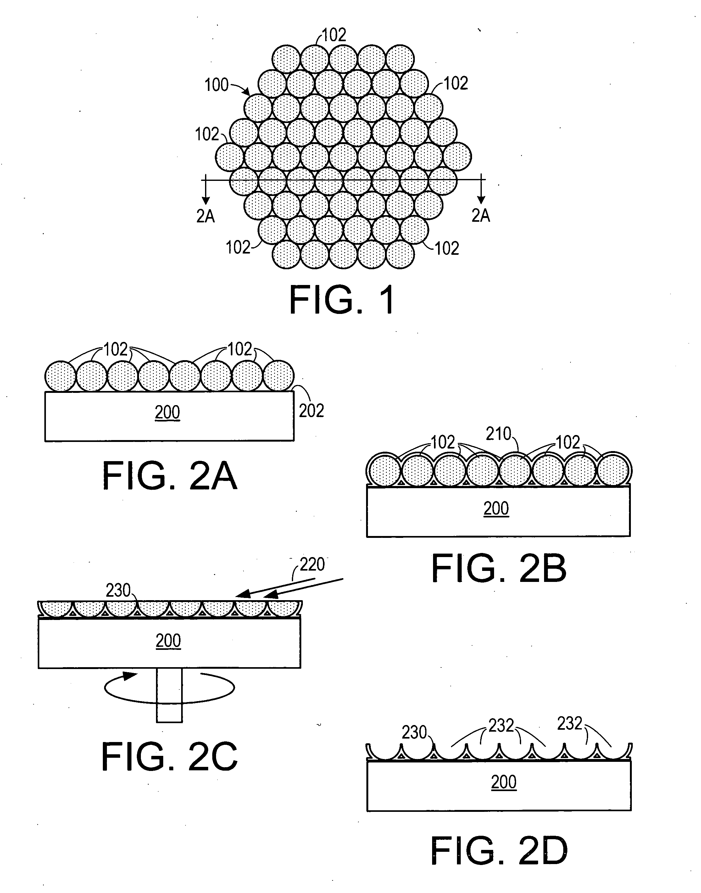
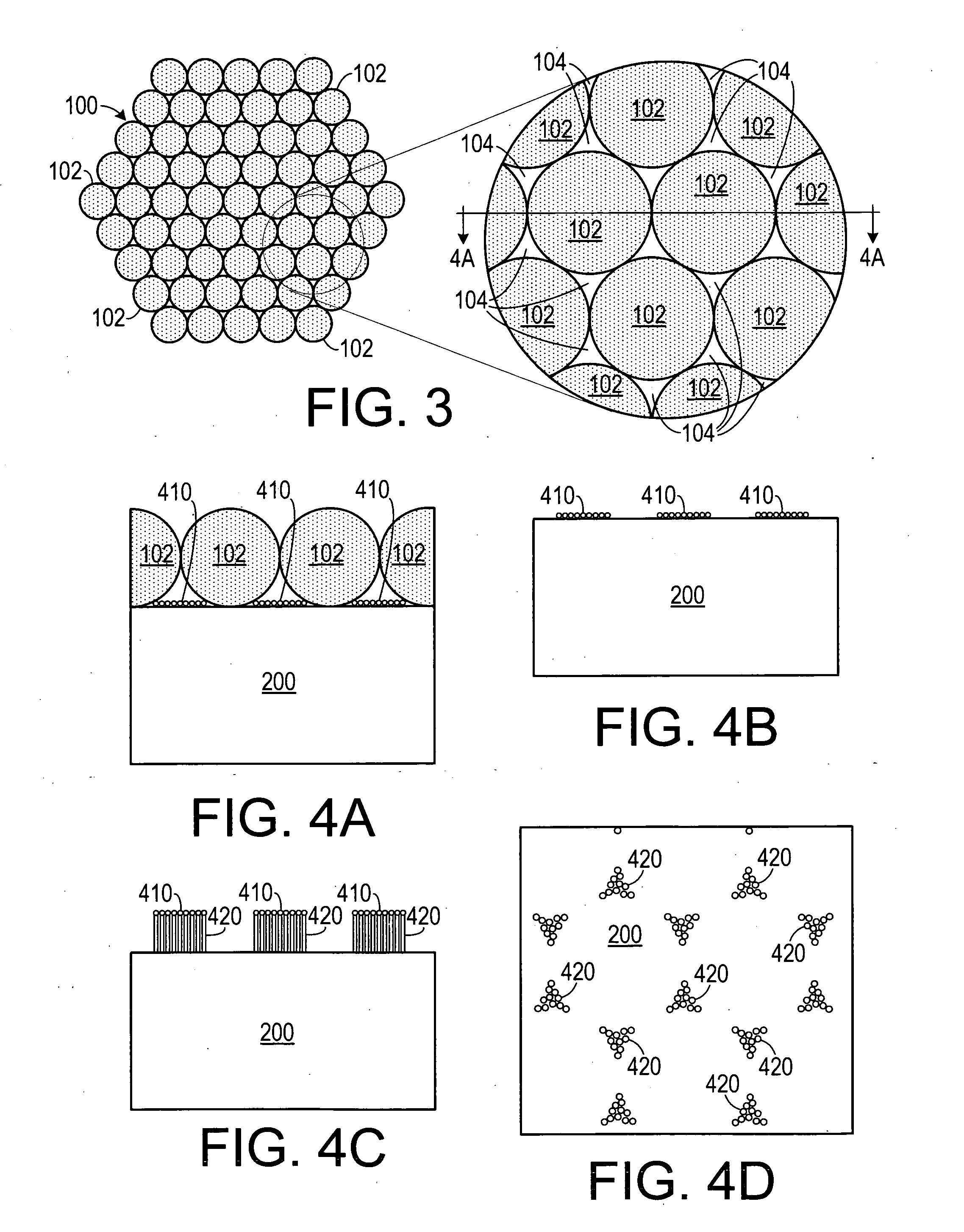
[0037] In one embodiment of the invention, a monolayer of organic spheres, such as polystyrene spheres, is self-assembled onto a substrate. As shown in FIG. 1, such a monolayer 100 includes a plurality of spheres 102 arranged in an close packing arrangement, such as a hexagonal arrangement. As shown in FIG. 2A, the spheres 102 form a monolayer on the top surface 202 of a substrate 200 (which could include a single crystal of aluminum oxide).

[0038] As shown in FIGS. 9A-9E, one way of creating the monolayer 914 on the substrate 912 starts with adding a p...


PUM


Abstract

A method of making nanostructures using a self-assembled monolayer of organic spheres is disclosed. The nanostructures include bowl-shaped structures and patterned elongated nanostructures. A bowl-shaped nanostructure with a nanorod grown from a conductive substrate through the bowl-shaped nanostructure may be configured as a field emitter or a vertical field effect transistor. A method of separating nanoparticles of a desired size employs an array of bowl-shaped structures.

Description

CROSS-REFERENCE TO A RELATED PROVISIONAL PATENT APPLICATION [0001] The present application claims priority on U.S. Provisional Patent Application Ser. No. 60 / 528,740, filed Dec. 11, 2003, the entirety of which is incorporated herein by reference.STATEMENT REGARDING GOVERNMENT RIGHTS [0002] This invention was made with Government support under Contract No. DMR-9733160, awarded by the National Science Foundation, and Contract No. ARO DAAD 19-01-0603, awarded by the U.S. Army, the United States Government therefore has certain rights in the invention.BACKGROUND OF THE INVENTION [0003] 1. Field of the Invention [0004] The present invention relates to nanostructures and, more specifically to patterned nanostructures. [0005] 2. Description of the Prior Art [0006] Binary semiconducting oxides often have distinctive properties and can be used as transparent conducting oxide (TCO) materials and gas sensors. Current studies of semiconducting oxides have been focused on two-dimensional films a...

Claims


Application Information

Patent Timeline
IPC IPC(8): G02B5/20H01J1/304H01J9/02H01L29/06H01L29/22
CPCB82Y10/00B82Y30/00G02B5/206H01J1/304H01J9/025H01L29/0665H01L29/0673H01L29/0676H01L29/22Y10S977/811Y10S977/712Y10S977/938
Inventor WANG, ZHONG L.SUMMERS, CHRISTOPHER J.WANG, XUDONGGRAUGNARD, ELTON D.KING, JEFFREY
Owner GEORGIA TECH RES CORP
Why Eureka
Try Eureka