

Magnetic memory device
a memory device and magnetic technology, applied in the field of magnetic memory devices, can solve the problems of not being suitable for shielding, neither the size of the package nor the size of the magnetic shielding layer is found in any conventional technique, and achieves the effect of reducing the shielding effect, facilitating in-plane orientation, and careful consideration of the shield area
- Summary
- Abstract
- Description
- Claims
- Application Information
AI Technical Summary
Benefits of technology
Problems solved by technology
Method used
Image

Examples
Embodiment Construction
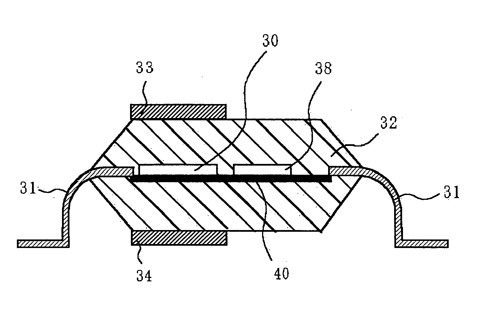
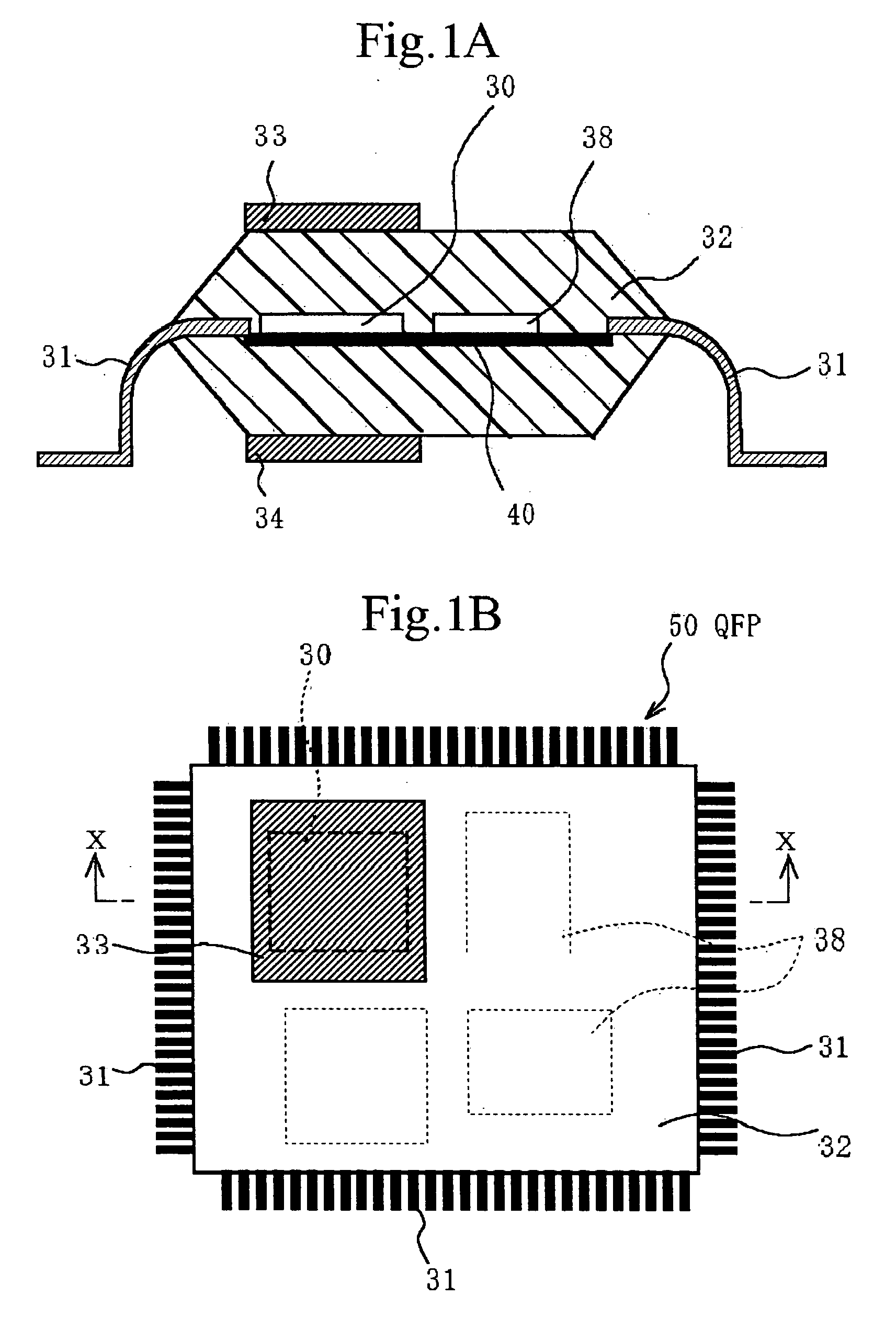
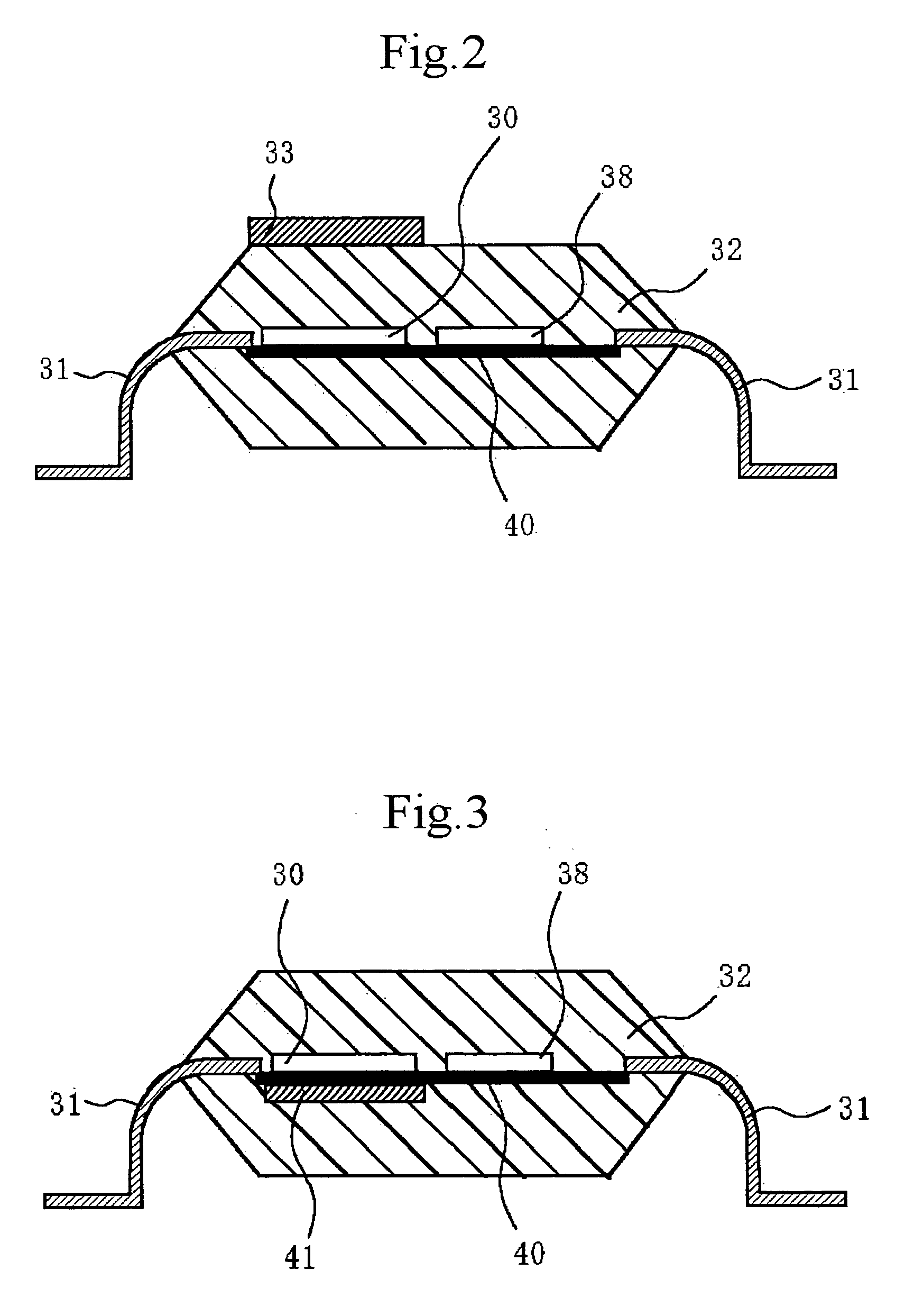
[0052] In the first and second magnetic memory devices of the present invention, for effectively exhibiting a magnetic shielding effect, it is preferred that the magnetic shielding layer is disposed on the top portion and / or bottom portion of a package of the memory element, or / and in a package of the memory element at the upper portion and / or lower portion as viewed from the memory element.
[0053] It is preferred that the magnetic shielding layer is constituted by a soft magnetic material which includes a soft magnetic material having high saturation magnetization and high magnetic permeability and containing at least one member selected from Fe, Co, and Ni, for example, a soft magnetic material having high saturation magnetization and high magnetic permeability, such as Fe, FeCo, FeCoV, FeNi, FeSiAl, FeSiB, or FeAl.
[0054] In the second magnetic memory device of the present invention, when the memory element is mounted on a substrate, together with another element, such as a DRAM,...
PUM
 Abstract
Description
Claims
Application Information