Method and device for performing cache reading

a cache and reading technology, applied in memory systems, memory adressing/allocation/relocation, instruments, etc., can solve the problems of large layout area, relative complexity structurally, and/or slowness, and achieve the effect of reducing data transfer tim

Active Publication Date: 2005-10-13
SAMSUNG ELECTRONICS CO LTD
View PDF8 Cites 59 Cited by
  • Summary
  • Abstract
  • Description
  • Claims
  • Application Information

AI Technical Summary

Benefits of technology

[0018] Example embodiments of the present invention are directed to semiconductor devices, such as semiconductor memory devices, including, for example, flash memory, with reduced data transfer time.
[0019] Example embodiments of the present invention are directed to programming methods with reduced data transfer time.
[0025] In example embodiments, the present invention is directed to a semiconductor device including a controller for overlapping at least two of tR, tT, and tH to reduce a total transfer time between the semiconductor device and a host device, where tR is a read operation time, tT is a buffer transfer time, and tH is a host transfer time.

Problems solved by technology

Non-volatile memory does not lose data when power is lost, but generally does not permit random access and is generally slower than volatile memory.
The page buffers of FIGS. 5a-6 may perform interleave operations, but also may be relatively complex structurally, have a relatively large layout area, and / or be relatively slow.

Method used


Image

  • Method and device for performing cache reading
  • Method and device for performing cache reading
  • Method and device for performing cache reading

Examples


Embodiment Construction

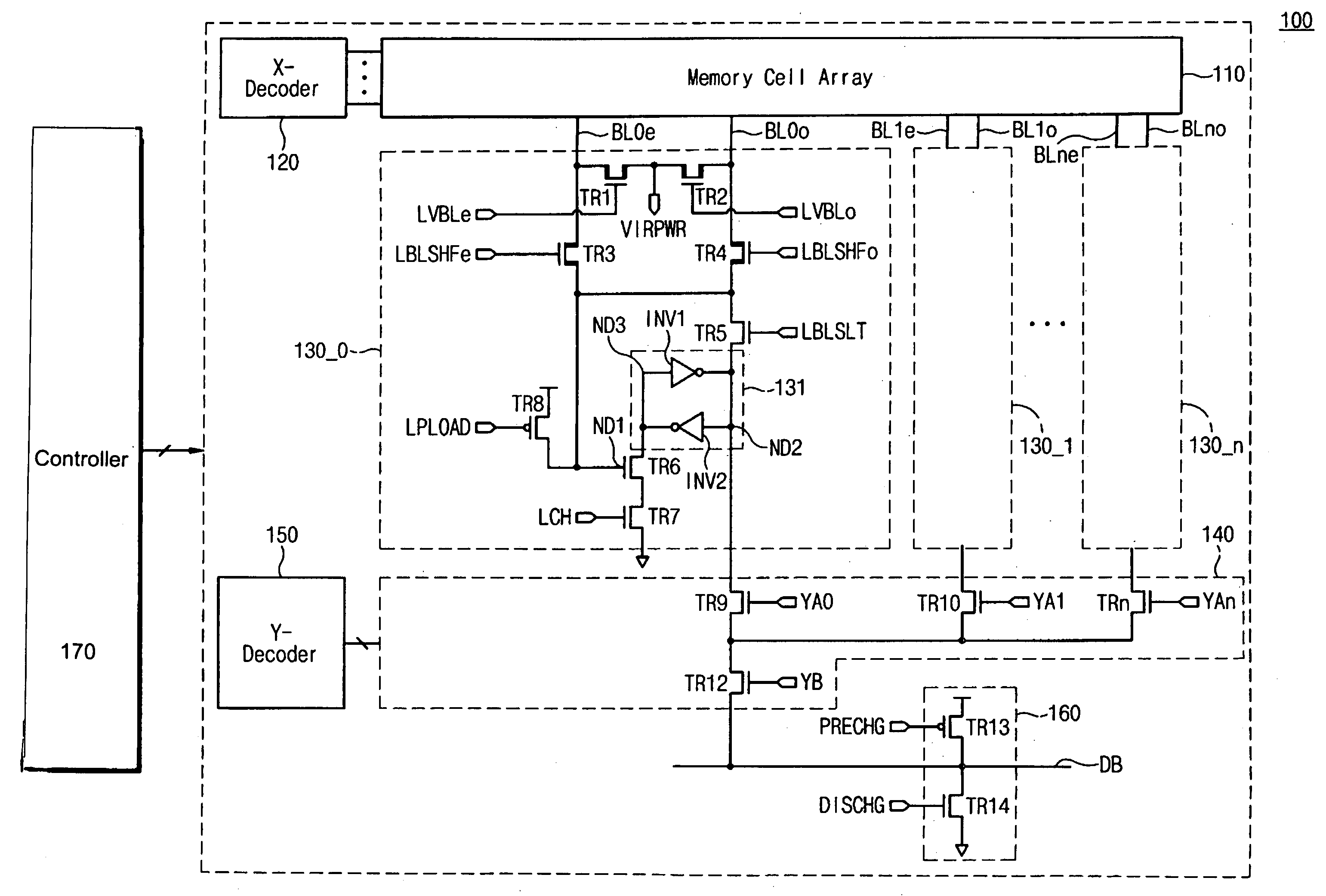
[0051] In example embodiments, the present invention is directed to a method and device for performing a cache operation, for example, a cache read operation.

[0052] In example embodiments, the present invention is directed to a method and device for reducing a data transfer time.

[0053] In example embodiments, the present invention is directed to a method and device for overlapping at least two of tR, tT, and tH to reduce a total transfer time where tR is a read operation time, tT is a buffer transfer time, and tH is a host transfer time.

[0054] In example embodiments, the present invention is directed to a method and device for transferring data where the data includes n pages of data (where n is an integer), and the total transfer time is less than n*(tR+tT+tH).

[0055] In example embodiments, the present invention is directed to a method and device for transferring data where the data includes n pages of data (where n is an integer), and the total transfer time is less than or eq...


PUM


Abstract

Method and device for reading data from a semiconductor device, where tR is a read operation time, tT is a buffer transfer time, and tH is a host transfer time, where at least two of tR, tT, and tH may be overlapped to reduce a total transfer time.

Description

PRIORITY STATEMENT [0001] This application claims the benefit under 35 U.S.C. § 119(a) of Korean Patent Application No. 2004-21654 filed on Mar. 30, 2004, the contents of which are hereby incorporated by reference in their entirety. BACKGROUND OF THE INVENTION [0002] Recent developments in memory applications, such as mass storage, code memory, and other multimedia applications increasingly require memory devices with higher density. Mass storage applications may include memory cards (for example, for mobile computers), solid-state memory (for example, sturdy and / or reliable storage disks), digital cameras (for recording still or moving images and sound), and voice or audio recorders for recording near CD quality sound). [0003] Code memory applications may include basic input / output systems (BIOS) or network applications (for example, memory in a personal computer, other terminal, router, or hub), telecommunications applications (for example, switches), mobile phone applications (fo...

Claims


Application Information

Patent Timeline
Patent Type & Authority Applications(United States)
IPC IPC(8): G06F12/00G11C16/02G06F12/08G11C7/00G11C7/10G11C11/34G11C11/409G11C11/419G11C16/00G11C16/04G11C16/06G11C16/26
CPCG06F12/0893G11C7/1039G11C7/1051G11C2207/2245G11C16/0483G11C16/26G11C7/106H02K5/24H02K5/10
Inventor LEE, JIN-YUBHWANG, SANG-WON
Owner SAMSUNG ELECTRONICS CO LTD
Why Eureka
Try Eureka