Microarray based affinity purification and analysis device coupled with solid state nanopore electrodes

a nanopore electrode and affinity purification technology, applied in the field of microarrays, can solve the problems of increasing the cost of labeling, affecting the completion of assays, and affecting the accuracy of assays,

Inactive Publication Date: 2005-10-13
AGILENT TECH INC
View PDF11 Cites 86 Cited by
  • Summary
  • Abstract
  • Description
  • Claims
  • Application Information

AI Technical Summary

Problems solved by technology

Labeling is typically performed during a sample preparation process that can add significant time to the assay completion.
Secondly, the use of labels increases costs, and can potentially cross react with other molecules or probes.
Microarrays also suffer from the limitation that they can require multiple runs and may require extensive time to employ in an analysis.
In addition, they may be limited by hybridization parameters such as requiring a 20 mer or smaller to obtain complete hybridizations.
This blockage leads to a decrease in the ionic current flow of the buffer solution through the nanopore during the biopolymer translocation.
These initially proposed systems suffer from a number of problems.
Reprodu...

Method used


Image

  • Microarray based affinity purification and analysis device coupled with solid state nanopore electrodes
  • Microarray based affinity purification and analysis device coupled with solid state nanopore electrodes
  • Microarray based affinity purification and analysis device coupled with solid state nanopore electrodes

Examples


second embodiment

[0063] Referring now to FIGS. 7C and 7D, the invention, a series of separate substrates may be employed. For instance, a first substrate 12 and a second substrate 18 may be employed in place of the single substrate 8. In this embodiment of the invention, the first electrode 7 comprises first substrate 12 or a portion of this substrate. The electrode may be embedded, attached, layered, deposited, etched on the substrate or it may comprise all or a portion of the first substrate 12. Second electrode 9 comprises the second substrate 18 or a portion of the substrate. The electrode may be embedded, attached, layered, deposited, etched on the substrate or it may comprise all or a portion of the second substrate 18. The first substrate 12 is positioned adjacent to the second substrate 18. The figure shows the first substrate 12 positioned spatially above the second substrate 18. The first electrode 7 may comprise a first nanopore 3 while the second electrode 9 may comprise a second nanopor...

third embodiment

[0064] Referring now to FIGS. 7E and 7F, the present invention is provided. In this embodiment, the first electrode 7 and the second electrode 9 are positioned in the same plane. One or more optional substrates or electrodes may be employed. When the optional substrate 8 is not employed, the first electrode 7 and the second electrode 9 may be positioned adjacent to the nanopore 3. Although the figures show a pair of electrodes, the invention should not be interpreted to be limited to only this configuration. Various electrodes of varying shapes or sizes may be employed. Furthermore, it is anticipated that the invention comprises a number of similar or different electrodes capable of tunneling in a variety of directions and space (i.e. one, two and three dimensional space).

[0065] Referring now to FIG. 7G another embodiment of the present invention is shown. FIG. 7G illustrates a cross-sectional detail of an embodiment 300 of the present invention. Embodiment 300 is an embodiment in w...

embodiment 300

[0066] As seen in FIG. 7G, embodiment 300 comprises a nanopore 308 that is wide near its lower end and narrow near its upper end. Membrane 306 comprises a region of a material such as silicon dioxide, and the lower ring-shaped electrode 310 comprises a conductor such as platinum. Lower electrode 310 is formed in a manner that surrounds the perimeter of nanopore 308. On top of lower electrode 310a lower insulator layer 312 is placed in a manner that surrounds the perimeter of nanopore 308 and leaves exposed a perimeter portion 330 of electrode 310. On top of lower insulator layer 312, an upper electrode 314 is formed in a manner that surrounds the perimeter of nanopore 308. On top of upper electrode 314 an upper insulator 316 is placed in a manner that surrounds the perimeter of nanopore 308 and leaves exposed a perimeter portion 332 of electrode 314. Hole 326 in top insulator 328 provides access to the upper end of the nanopore for a biopolymer molecule 334 represented schematically...


PUM

PropertyMeasurementUnit
Lengthaaaaaaaaaa
Nanoscale particle sizeaaaaaaaaaa

Abstract

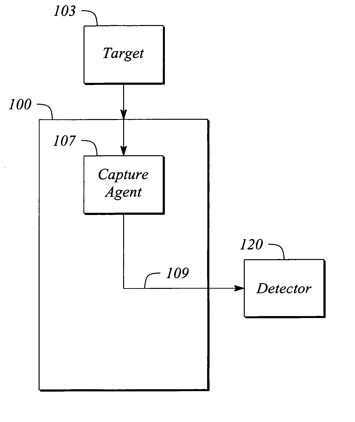
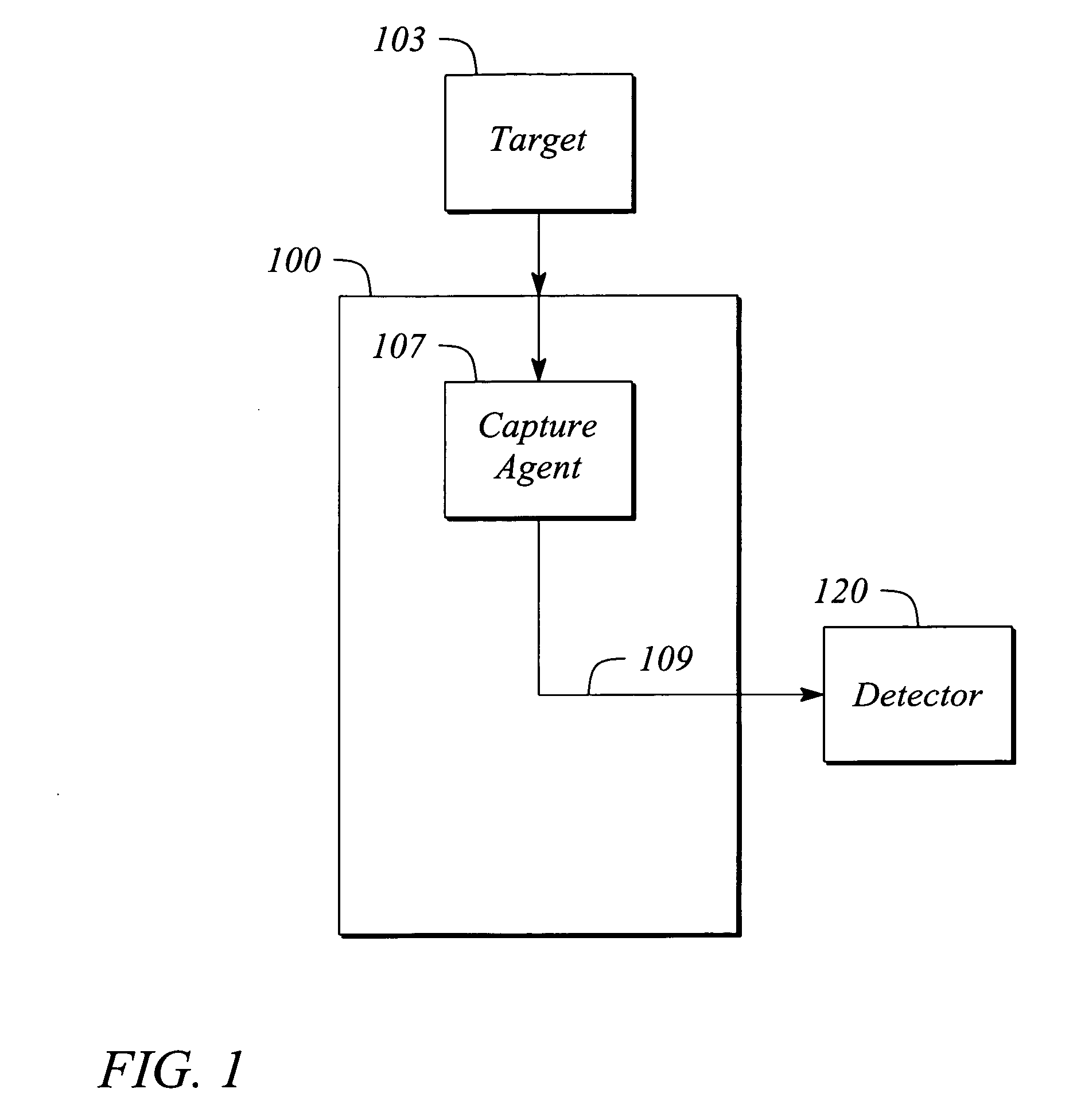
An apparatus and method for separating and identifying chemical moieties. The apparatus employs a microarray device coupled to a nanopore system. The apparatus both separates and identifies target molecules without the requirement of extraneous tags or fluorescent markers. Methods for using the apparatus are also disclosed.

Description

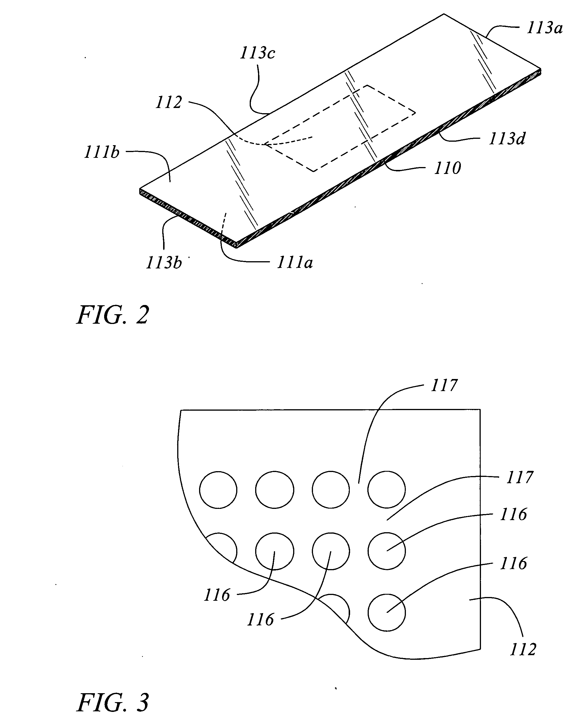
FIELD OF THE INVENTION [0001] The invention relates to the field of microarrays and more particularly to an apparatus and method for separating, identifying and quantitating chemical moieties using arrays. BACKGROUND OF THE INVENTION [0002] Polynucleotide arrays (such as DNA or RNA arrays) are known and are used, for example, as diagnostic or screening tools. Such arrays include regions of usually different sequence polynucleotides arranged in a predetermined configuration on a substrate. These regions (sometimes referenced as “features”) are positioned at respective locations (“addresses”) on the substrate. In use, the arrays, when exposed to a sample, will exhibit an observed binding or hybridization pattern. This binding pattern can be detected upon interrogating the array. For example, all polynucleotide targets (for example, DNA) in the sample can be labeled with a suitable label (such as a fluorescent dye), and the fluorescence pattern on the array accurately observed followin...

Claims


Application Information

Patent Timeline
IPC IPC(8): C12M1/34C12Q1/68
CPCC12Q1/6825C12Q1/6816C12Q2565/631C12Q2565/607C12Q2565/501G01N33/48721
Inventor JOYCE, TIMOTHY H.
Owner AGILENT TECH INC
Why Eureka
Try Eureka