Light emitting diode and process for producing the same

Inactive Publication Date: 2005-10-20
PEARL LAMP WORKS +1
View PDF7 Cites 1 Cited by
  • Summary
  • Abstract
  • Description
  • Claims
  • Application Information

AI Technical Summary

Benefits of technology

[0025] Preferably, the step of filling the cationic polymerization type transparent epoxy resin in the light emitting diode making method of the present invention includes a step of engaging the lead in a groove formed in an upper end face of the casing; a step of filling a light curable epoxy resin in the groove, in which the lead is engaged, to the upper end face of the casing, irradiating the light curable epoxy resin with ultraviolet rays of light to thereby fix the lead in the groove in the casing, and a step of filling the cationic polymerization transparent epoxy resin to a level flush with the upper end face of the casing. In the present invention, by means of those steps, leakage of the resin can be completely avoided.
[0026] Also preferably, the step of filling the cationic polymerization type transparent epoxy resin in the light emitting diode making method of the present invention includes a step of engaging the lead in a groove formed in an upper end face of the casing; a step of covering the casing with a frame for covering the upper end face of the casing and having a projection at a location corresponding to or aligned with the groove in the casing; and a step of filling the cationic polymerization type transparent resin to a level flush with the upper end face of the casing. By those process steps, leakage

Problems solved by technology

However, with the light emitting diode having the structure in the first example, in which the metallic reflecting surface is provided outside the casing, since the light emitting diodes are packaged for shipping with the reflecting surfaces exposed to the outside, even though the protective layer is employed in the form of a hard coating, contact between the reflecting surfaces and contact between the reflecting surface and tips of the leads will often bring about flaws appearing on the reflecting surface having been passed through the protective (hard coating) layer during surface mounting or handling of the light emitting diodes after being unpackaged.
Because of the flaws, there have been problems in that the reflecting performance of the reflecting surface tends to be lowered and the reflecting surface tends to be deteriorated quickly.
Accordingly, when the light emitting diode having the above described metallic reflecting surface is surface mounted on the circuit board and is passed through the solder reflow furnace, the circuit board including the light emitting diode is naturally heated to a temperature about equal to 250° C. As such, wrinkling and/or cracking may occur in the reflecting surface due to the difference in coefficient of thermal expansion between the transparent epoxy resin and the silver or aluminum metallic layer forming the reflecting surface, accompanied by reduction in reflectivity of th

Method used


Image

  • Light emitting diode and process for producing the same
  • Light emitting diode and process for producing the same
  • Light emitting diode and process for producing the same

Examples


Embodiment Construction

[0037] Hereinafter, a preferred embodiment of the present invention will be described in detail with particular reference to FIGS. 1 to 5.

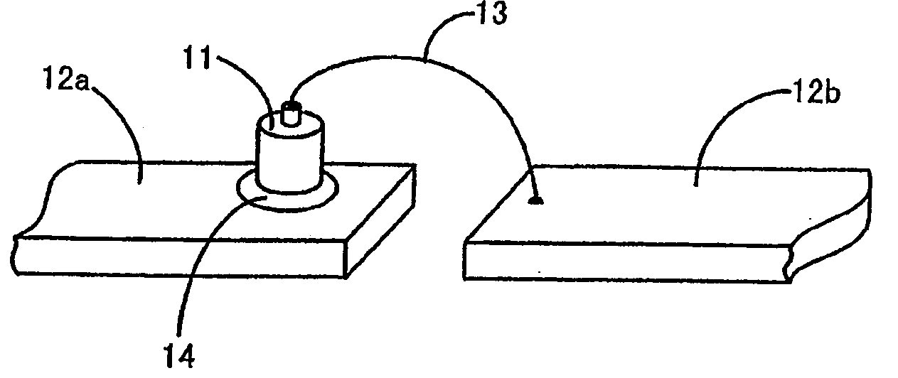
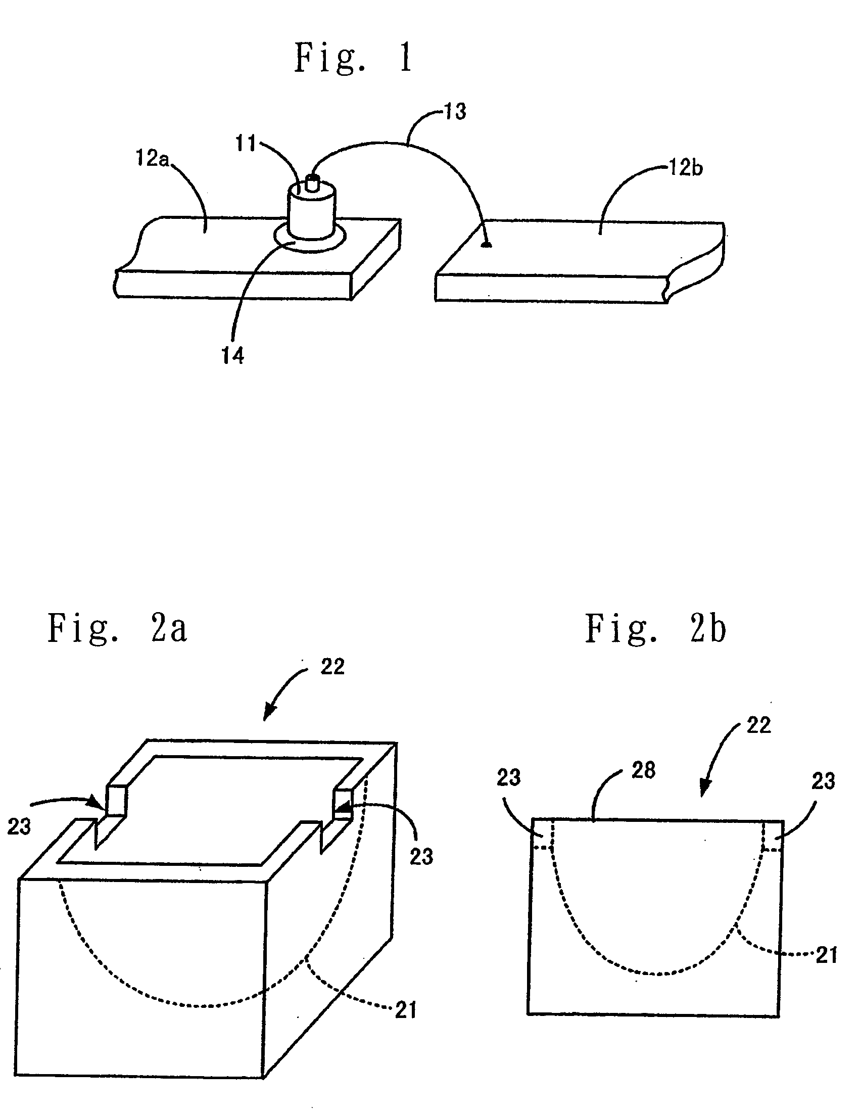
[0038]FIG. 1 illustrates a schematic diagram used to explain a light emitting element mounted on a lead used in a light emitting diode according to the present invention. The light emitting element 11 is rigidly connected at one end with a lead 12a by means of an electroconductive bonding agent 14 and at the opposite end with a lead 12b through a gold wire 13. The light emitting element so connected with the leads is prepared in readiness for the practice of the present invention.

[0039]FIGS. 2a and 2b illustrate a schematic perspective view and a schematic side view of a casing used in the light emitting diode of the present invention. As shown in FIGS. 2a and 2b, the casing 22 is made of a synthetic resin in its entirety and is formed with a concave cavity defining a concave surface which is in turn vapor deposited with a plated layer of alumin...


PUM


Abstract

A light emitting diode includes a casing having a concave surface, a reflecting surface formed by depositing a metallic layer on a concave surface thereof, and a lead having a light emitting element fitted thereto so as to confront the reflecting surface. A cationic polymerization type transparent epoxy resin is filled within a cavity of the casing having the concave surface, and the resin is hardened while the resin, the reflecting surface and the casing form a sandwich structure. With this construction, the light emitting diode is provided, in which neither wrinkling nor cracking occur in the reflecting surface. In addition, there is no possibility of the reflecting surface being flawed during the handling and transportation. Also, even in a reflow furnace operation in which a soldering is carried out, thermal deformation including formation of wrinkling and cracking in the reflecting surface can be completely avoided. Yet, since the cationic polymerization type transparent epoxy resin has so low a rate of shrinkage after hardening that the planarity of a light radiating surface after the hardening can be maintained and, for this reason, rays of light emerging from the light radiating surface can be emitted to the outside without being refracted at the interface between the light radiating surface and the outside.

Description

FIELD OF THE INVENTION [0001] The present invention relates to a light emitting diode having a reflecting surface covered by a cationic polymerization transparent epoxy resin, which is a kind of a hardening accelerating epoxy resin, and a method of making the same. BACKGROUND ART [0002] The structure of a light emitting diode for effectively radiating rays of light, emitted from a light emitting element, outwardly frontward through a metallic reflecting surface is disclosed in numerous patent publications. In those prior arts, the structure can be classified into three types including a first type in that the metallic reflecting layer is vapor deposited on an outside of the casing, a second type in that the metallic reflecting layer is vapor deposited on an inside of the casing, and a third type in that the metallic reflecting layer pre-manufactured is employed. [0003] As a first example in which the metallic reflecting layer is formed on an outside of the casing, light emitting dio...

Claims


Application Information

Patent Timeline
IPC IPC(8): H01L33/46H01L33/56H01L33/60H01L33/62
CPCH01L33/60H01L33/54H01L2224/32245H01L2224/48091H01L2224/48247H01L2224/73265H01L2224/45144H01L2924/181H01L2924/00014H01L2924/00H01L2924/00012
Inventor YAMAZAKI, SHIGERU
Owner PEARL LAMP WORKS
Why Eureka
Try Eureka