Method and apparatus for protecting a gate oxide using source/bulk pumping

a gate oxide and source/bulk pumping technology, applied in the field of circuits, can solve the problems of limiting the gate-to-source and/or gate-to-bulk voltage produced by the esd event, and achieve the effect of reducing the risk of overvoltage protection resistan

Active Publication Date: 2005-10-20
SOFICS BVBA
View PDF3 Cites 18 Cited by
  • Summary
  • Abstract
  • Description
  • Claims
  • Application Information

AI Technical Summary

Benefits of technology

[0010] The present invention is a method and apparatus for limiting the gate-to-source and / or gate-to-bulk voltage by pumping either the bulk and / or source in response to an ESD event. The apparatus comprises a protection circuit that, in response to an ESD event, limits the voltage formed between two terminals of a transistor by adjusting a potential level on the second terminal. In one embodiment of the invention, an electrical signal resulting from an ESD event is coupled from a transistor gate terminal experiencing the event to an impedance circuit connected to the source and / or bulk of the transistor. The voltage produced across the impedance circuit raises the potential level of the source and / or bulk, thus limiting the gate-to-source and / or gate-to-bulk voltage produced by the ESD event.

Problems solved by technology

The voltage produced across the impedance circuit raises the potential level of the source and / or bulk, thus limiting the gate-to-source and / or gate-to-bulk voltage produced by the ESD event.

Method used


Image

  • Method and apparatus for protecting a gate oxide using source/bulk pumping
  • Method and apparatus for protecting a gate oxide using source/bulk pumping
  • Method and apparatus for protecting a gate oxide using source/bulk pumping

Examples


first embodiment

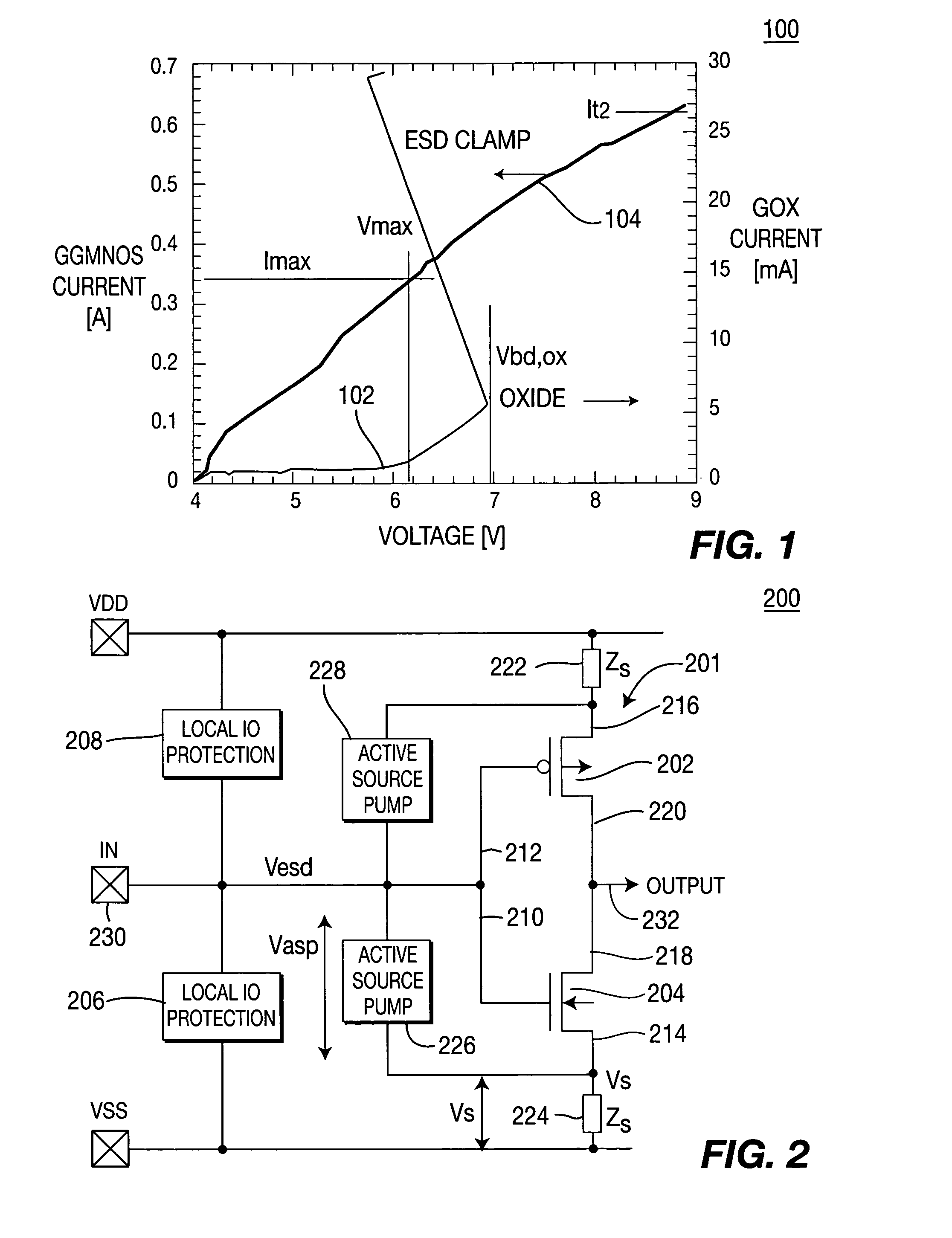
[0028]FIG. 2 depicts a block diagram of a circuit 200 that performs source pumping in accordance with the present invention. The circuitry 201 to be protected from ESD events comprises transistors 202 and 204, e.g., a traditional input signal inverter. These transistors may be NMOS or PMOS type transistors. Of course, the present invention can be used with other circuit configurations, devices or individual transistors.

[0029] A first conventional ESD clamp circuit 206 (also referred to herein as a primary protection circuit) is formed between the IN terminal and Vss, and a second conventional ESD clamp circuit 208 is formed between the IN terminal and Vdd. For example, such circuits include those described in commonly assigned U.S. Pat. Nos. 6,768,616 and 6,791,122 which are herein incorporated by reference. Each transistor 202 and 204 comprises a gate 212 / 210, a source 216 / 214, and a drain 220 / 218. Vdd is coupled to the source 214 of transistor 202 via a first source impedance circ...

second embodiment

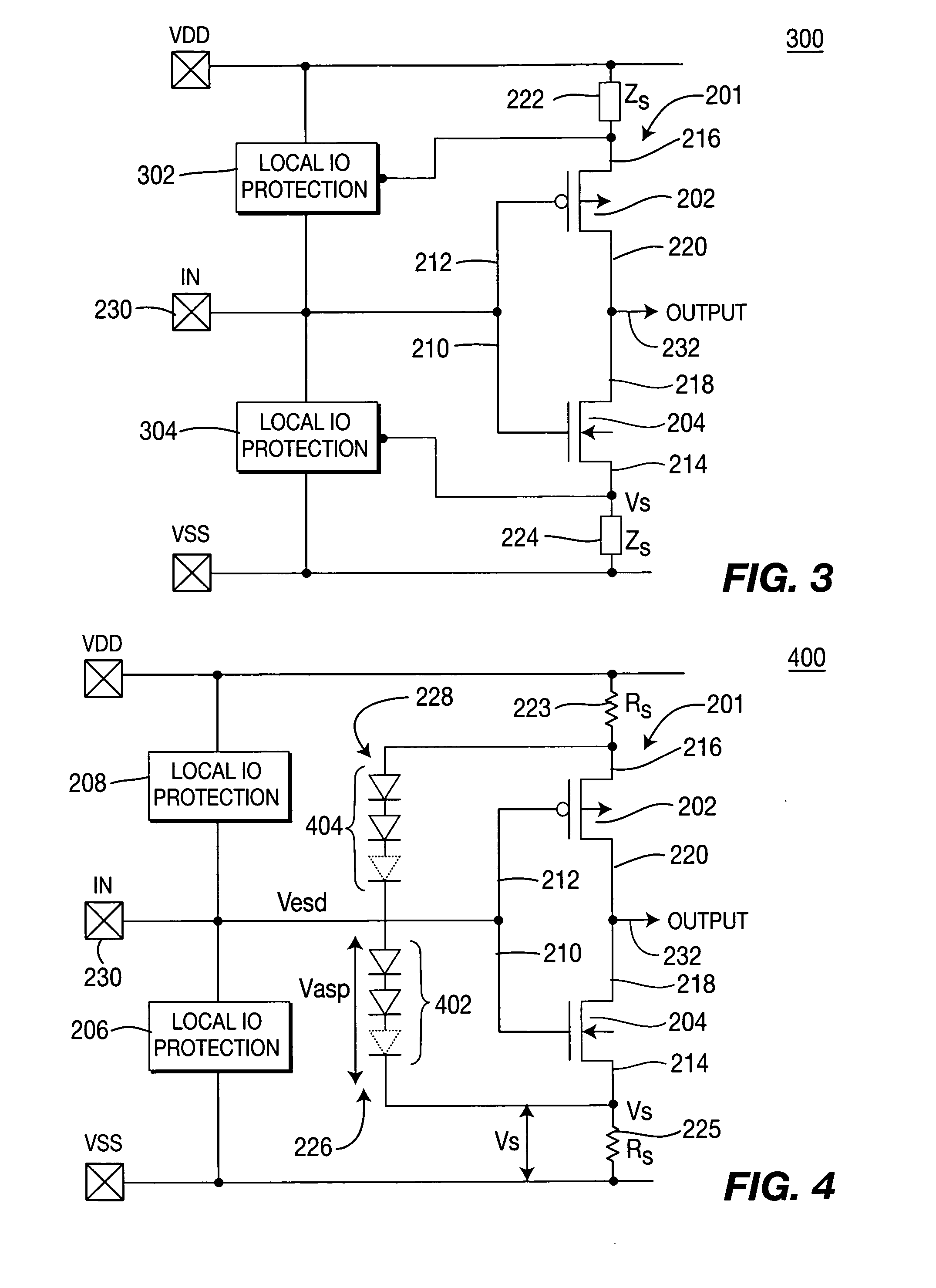
[0030]FIG. 3 depicts a block diagram of a circuit 300 that forms the invention, wherein the source pumping voltage is supplied by each of the primary protection circuits 302 and 304. In other words, the source pumps 226 and 228 of FIG. 2 are embedded into the ESD clamp circuits 302 and 304.

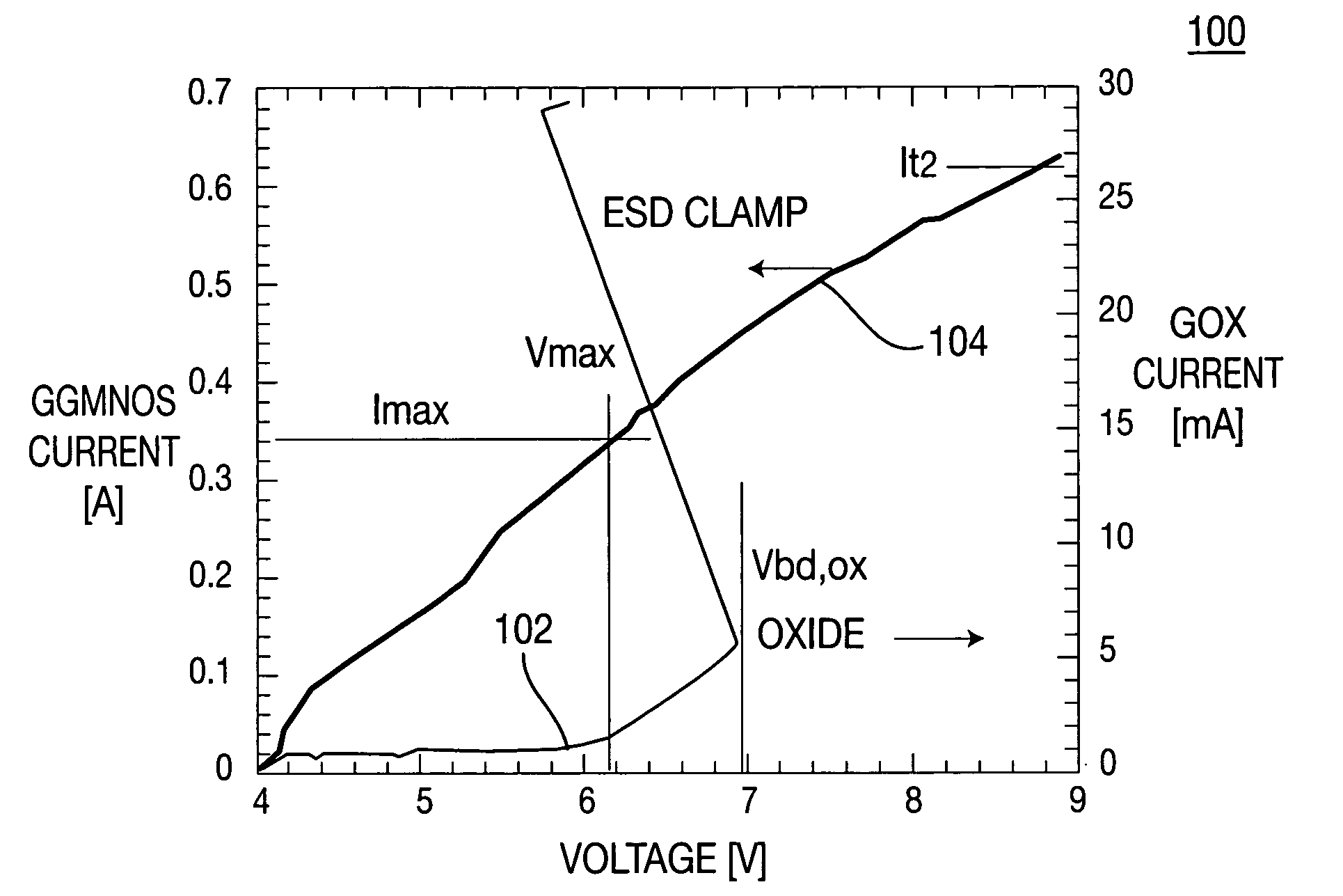
[0031] In either embodiment, during an ESD stress event, the source impedance circuits 222 / 224 provide a voltage drop to lift the source potential by pumping a small amount of ESD current (typically 214 / 216. A small fraction of the ESD current is conducted thru the source impedance ZS 222 / 224 that, in turn, results in a source bias voltage VS. In other words, the total ESD voltage occurring between pad and ground is divided into two parts: VESD=VASP+VS. As a result, a higher total transient gate voltage VESD=Vmax′ can be tolerated before the low ESD voltage limit Vmax (close to the transient oxide breakdown) directly across the gate oxide (GOX) is reached. In other words, the effective ESD design ...

third embodiment

[0047]FIG. 8 depicts a block diagram of the invention. The general concept of this embodiment is to create a potential increase at the internal source node due to the tunneling current flowing through the gate-source oxide during ESD without using any external pump current. Prerequisite for a functional design, however, is that the source series resistance 806 / 808 can be switched from a relatively low-ohmic normal operation state (Rs˜10 Ω) to high-ohmic ESD value (Rs>˜kΩ). Suitable Rs elements 806 / 808 as well as control circuits 802 / 804 are required. The control circuits 802 / 804 detect the ESD event and turn the active Rs device 806 / 808 into the high-resistance ESD mode, thus increasing the internal source voltage and allowing for a higher ESD gate voltage Vg.

[0048]FIG. 9 depicts a first implementation of the third embodiment of the invention shown in FIG. 8. A normally-on PMOS transistor 902 is connected in series with the NMOS input transistor 204. A control circuit 802 comprising...


PUM


Abstract

A method and apparatus for providing ESD event protection for a circuit using a source or bulk pump to increase the bulk and/or source potential level during an ESD event. The apparatus comprises a protection circuit that, in response to an ESD event, limits the voltage formed between two terminals of a transistor by adjusting a potential level on the second terminal.

Description

CROSS-REFERENCE TO RELATED APPLICATIONS [0001] This application claims benefit of U.S. provisional patent applications Ser. No. 60 / 555,566, filed Mar. 23, 2004, and Ser. No. 60 / 610,905, filed Sep. 17, 2004, both are herein incorporated by reference.BACKGROUND OF THE INVENTION [0002] 1. Field of the Invention [0003] The present invention generally relates to circuits that provide electrostatic discharge protection, and more particularly, to a method and apparatus for protecting a gate oxide using source / bulk pumping. [0004] 2. Description of the Background Art [0005] The protection of an ultra-thin gate oxide against electrostatic discharge (ESD) stress is a critical factor in obtaining sufficiently high levels of ESD hardness in advanced CMOS technologies. When the voltage applied to a gate oxide becomes too high, the gate oxide will suffer from catastrophic damage, i.e., it will break down. Typically, SiO2 breaks down at electric field strengths of 6-9 MV / cm (DC). During ESD stress...

Claims


Application Information

Patent Timeline
Patent Type & Authority Applications(United States)
IPC IPC(8): H01L27/02H02H9/00H03K17/0812
CPCH03K17/08122H01L27/0251
Inventor MERGENS, MARKUS PAUL JOSEFDE RANTER, FREDERIC MARIE DOMINIQUECAMP, BENJAMIN VANVERHAEGE, KOEN GERARD MARIAJOZWIAK, PHILLIP CZESLAWARMER, JOHNKEPPENS, BART
Owner SOFICS BVBA
Why Eureka
Try Eureka