Methods and apparatus for transferring conductive pieces during semiconductor device fabrication

a technology of semiconductor devices and conductive pieces, applied in the direction of soldering apparatus, semiconductor/solid-state device details, manufacturing tools, etc., can solve the problems of improper solder ball registration at one or more vacuum holes, and the difficulty of vacuum-based arrangement plates suffering from several drawbacks

Inactive Publication Date: 2005-10-20
APPLIED MATERIALS INC
View PDF16 Cites 139 Cited by
  • Summary
  • Abstract
  • Description
  • Claims
  • Application Information

AI Technical Summary

Problems solved by technology

Vacuum-based arrangement plates suffer from several drawbacks.
Also, during transfer of solder balls to the arrangement plate, improper solder ball registration may occur at one or more vacuum holes of the arrangement plate due to vacuum leaks, contamination, moisture, etc.

Method used


Image

  • Methods and apparatus for transferring conductive pieces during semiconductor device fabrication
  • Methods and apparatus for transferring conductive pieces during semiconductor device fabrication
  • Methods and apparatus for transferring conductive pieces during semiconductor device fabrication

Examples


Embodiment Construction

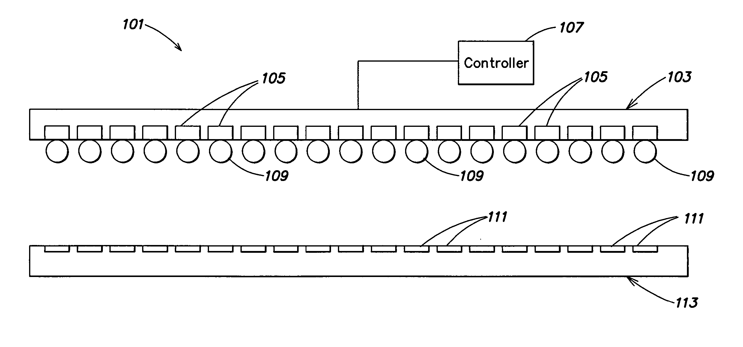
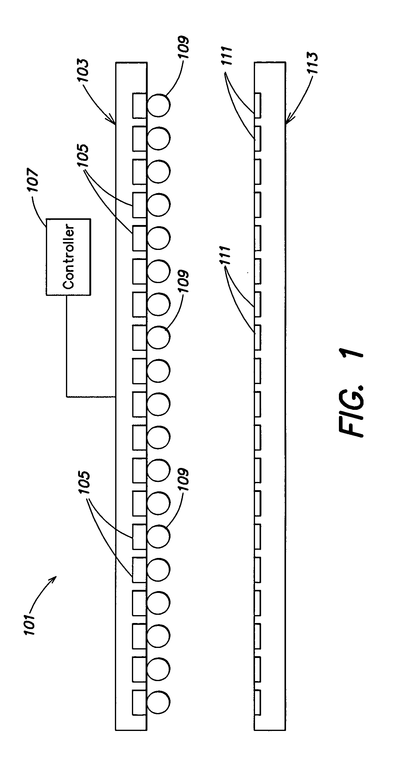
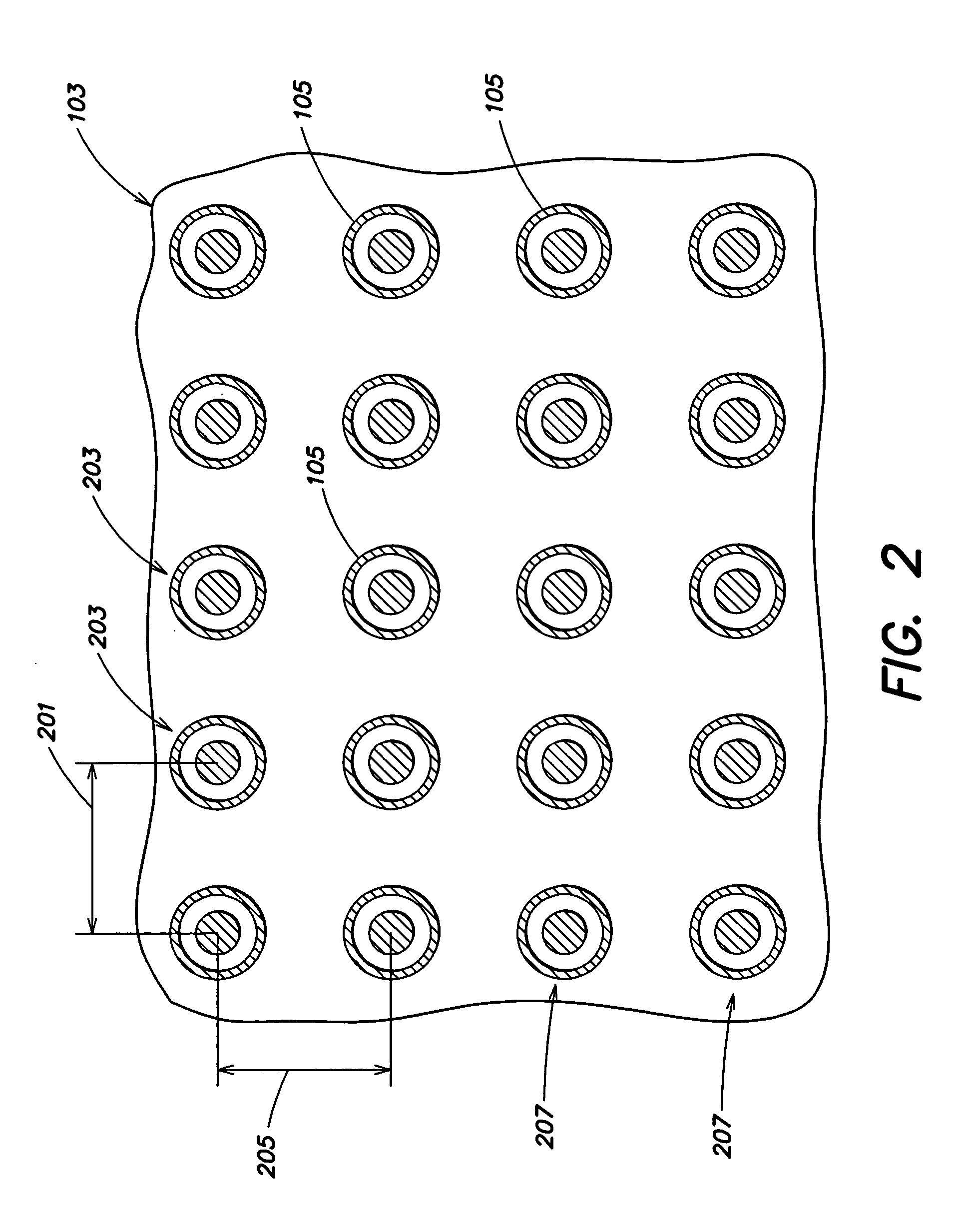
[0026]FIG. 1 is a schematic illustration of a conductive piece transfer apparatus 101 provided in accordance with the present invention. The conductive piece transfer apparatus 101 includes a transfer substrate 103 having a plurality electrodes 105 formed therein coupled to a controller 107. As will described further below, the electrodes 105 of the transfer substrate 103 are adapted to electrostatically hold conductive pieces, such as solder balls 109, solder cubes, solder cylinders or other similar materials or shapes, during transfer of the conductive pieces to electrode pads 111 of semiconductor devices (not separately shown) formed on a semiconductor wafer, glass plate, polymer substrate or similar device substrate 113. The transfer substrate 103 also may be employed to transfer conductive pieces to a printed circuit board or other carrier, as well as to individual substrate die.

[0027] The transfer substrate 103 may be fabricated on any suitable substrate such as a semiconduct...


PUM

PropertyMeasurementUnit
thicknessaaaaaaaaaa
thicknessaaaaaaaaaa
thicknessaaaaaaaaaa

Abstract

In a first aspect, a programmable transfer device is provided for transferring conductive pieces to electrode pads of a target substrate. The programmable transfer device includes (1) a transfer substrate; and (2) a plurality of individually addressable electrodes formed on the transfer substrate. Each electrode is adapted to selectively attract and hold a conductive piece during transfer of the conductive piece to an electrode pad of a target substrate. Numerous other aspects are provided.

Description

[0001] The present application claim priority to U.S. Provisional Patent Application Ser. No. 60 / 558,089, filed Mar. 31, 2004 and titled “METHODS AND APPARATUS FOR TRANSFERRING CONDUCTIVE PIECES DURING SEMICONDUCTOR DEVICE FABRICATION” (Attorney Docket No. 9073 / L), which is hereby incorporated by reference herein in its entirety.FIELD OF THE INVENTION [0002] The present invention relates to semiconductor device manufacturing, and more particularly to methods and apparatus for transferring conductive pieces during semiconductor device fabrication. BACKGROUND OF THE INVENTION [0003] During device packaging, electrical connections must be formed between semiconductor device electrode pads of a substrate die and package lead frames. One technique for forming such electrical connections is to employ a Flip Chip process. [0004] During a typical Flip Chip process, conductive bumps are provided at electrode pads of a substrate die, and the substrate die is attached to a circuit board or oth...

Claims


Application Information

Patent Timeline
Patent Type & Authority Applications(United States)
IPC IPC(8): B23K3/06B65G1/00H01L21/00H01L21/48H01L21/60H01L21/68H05K3/34
CPCH01L21/4853H01L21/67144H01L2924/1461H01L21/6835H01L23/544H01L24/11H01L24/742H01L2224/11003H01L2224/13099H01L2924/01004H01L2924/01013H01L2924/01033H01L2924/01051H01L2924/01057H01L2924/01074H01L2924/01078H01L2924/01079H01L2924/01082H01L2924/19041H01L2924/30105H05K3/3478H05K2201/10212H05K2203/0338H05K2203/041H01L2924/01006H01L2924/01023H01L2924/01068H01L2924/014H01L2224/11334H01L2924/00H01L2924/12042H01L2224/05573H01L2924/00014H01L2224/05599H01L21/68
Inventor RICE, MICHAEL R.BJORKMAN, CLAES H.ZHAO, JUNCOLLINS, KENNETH S.MIU, THOMAS
Owner APPLIED MATERIALS INC
Why Eureka
Try Eureka