Method and system for deciding a wiring route

Inactive Publication Date: 2005-10-20
HITACHI LTD
View PDF10 Cites 8 Cited by
  • Summary
  • Abstract
  • Description
  • Claims
  • Application Information

AI Technical Summary

Benefits of technology

[0006] It is therefore an object of the present invention to decide a wiring route drawing from a part eliminating intersections between wire connection relationships caused by the part direction and the terminal arrangement order, thereby reducing the wiring layer and increasing the mounting density.
[0010] According to the present invention, it is possible to align the bus wiring characteristics by eliminating the intersections between the wire connection relationships and to increase the wiring density. Thus, it is possible to reduce the wiring layer used and reduce the production cost.

Problems solved by technology

Accordingly, in the conventional method, there is a possibility that an appropriate wiring result cannot be obtained when performing a wiring under the condition that no through hole is used for a signal for which the wiring characteristic such as a bus should be aligned.
In this case, even by controlling the wiring order as shown in the right diagram of FIG. 2, it is difficult to align the wiring pattern.

Method used


Image

  • Method and system for deciding a wiring route
  • Method and system for deciding a wiring route
  • Method and system for deciding a wiring route

Examples


embodiment 1

(1) Embodiment 1

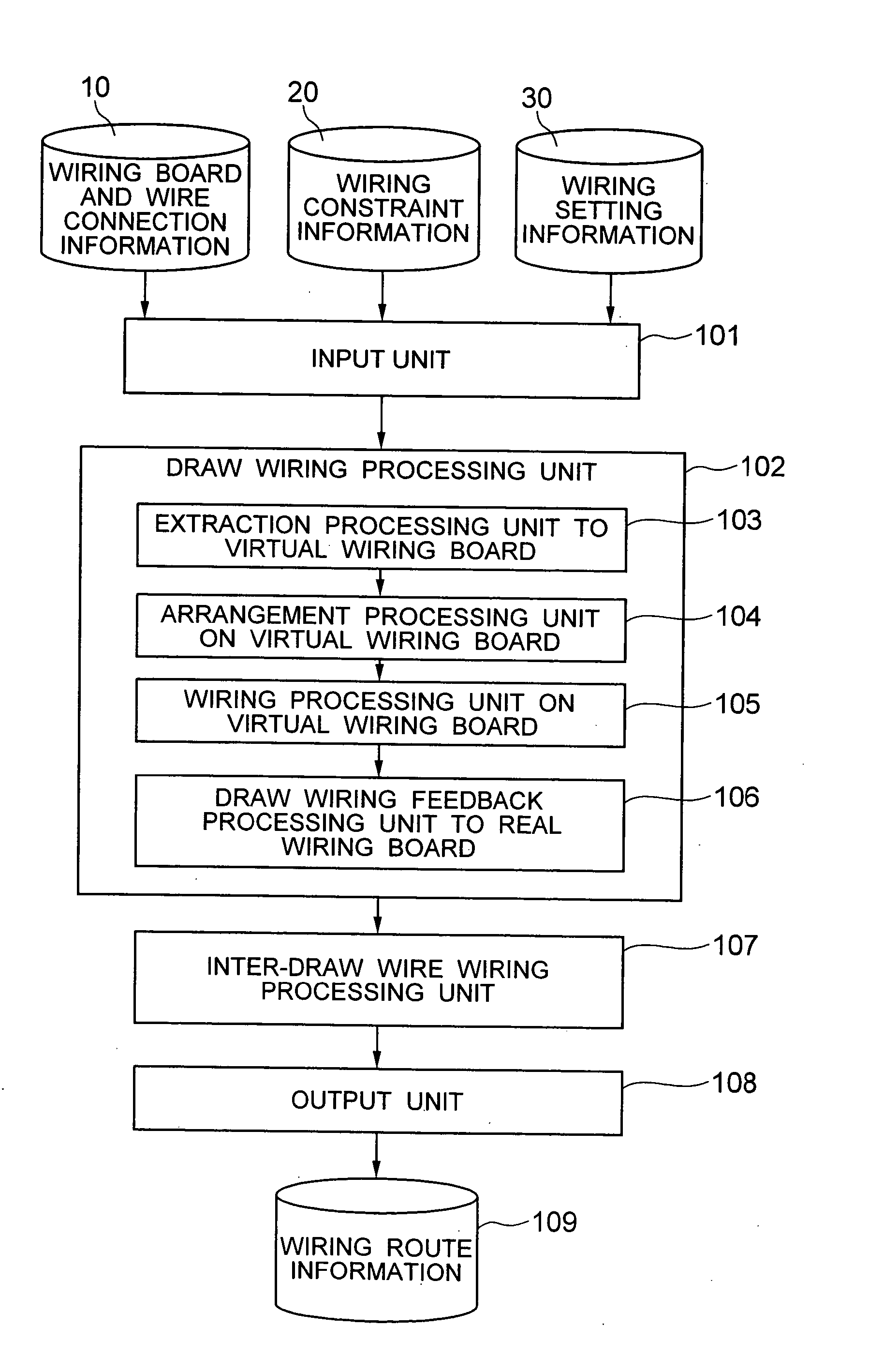
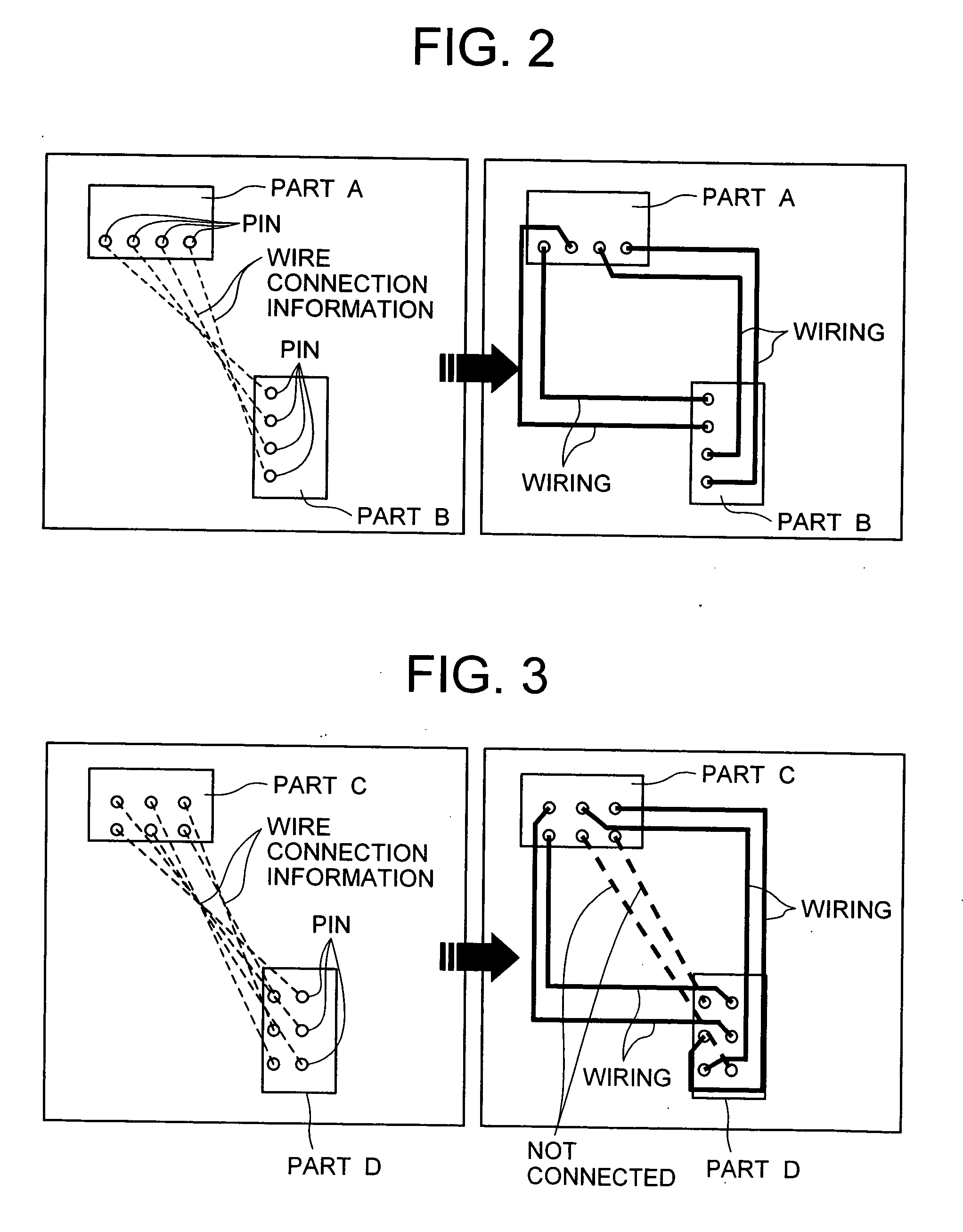
[0029]FIG. 1 shows a procedure of the method for deciding a wiring route according to the first embodiment of the present invention. An input unit 101 is used to receive: wiring board and wiring connection information 10 such as a wiring board shape, a wiring inhibited area, a part shape, part position information, pin position information, inter-pin connection information (hereinafter, referred to as connection information); wiring constraint information 20 such as bunch signal information, wiring width, wiring interval length, pair wiring instruction, and wiring inhibited information on wiring using a through hole; and wiring setting information 30 required when performing draw wiring processing such as a wiring margin area and wiring order information when performing draw wiring processing.

[0030] A draw wiring processing unit 102 is used to perform drawing of a wire from a pin to a part periphery boundary (hereinafter, referred to as draw wiring) by using a virtu...

embodiment 2

(2) Embodiment 2

[0047]FIG. 10 is a flowchart for displaying and correcting the result on the virtual wiring board by using the virtual wiring board display / instruction unit 1005 according to a second embodiment of the present invention. 1001 corresponds to the draw wiring processing unit 102 of the first embodiment shown in FIG. 1. Explanation will be given on this draw wiring processing.

[0048] An extraction processing unit 1002 to the virtual wiring board, an arrangement processing unit 1003 on the virtual wiring board, a wiring processing unit 1004 on the virtual wiring board, and a draw wiring feedback processing unit 1006 to the real wiring board are equivalent to 103, 104, 105, and 106 explained in the first embodiment, respectively.

[0049]1005 denotes a virtual wiring board display / instruction unit for displaying the wiring result by the draw wiring processing unit 1004 on the virtual wiring board. Moreover, for the display result, 1005 corrects the arrangement position and t...

embodiment 3

(3) Embodiment 3

[0054]FIG. 112 shows a system configuration according to a third embodiment of the present invention. The first embodiment and the second embodiment are examples in which the draw wiring result on the virtual wiring board is fed back to the real wiring board (106) and then wiring processing between the draw wires is performed on the real wiring board (107). However, it is possible to provide a system not performing the wiring between the draw wires (107). In this case, the wiring between the draw wires may be performed by using an ordinary wiring processing tool.

[0055]1201 denotes an input unit which receives wiring board and wire connection information 10, wiring constraint information 20 and wiring setting information 30.

[0056]1202 denotes a draw wiring processing unit which includes the following five processing units: an extraction processing unit 1203 to the virtual wiring board, an arrangement processing unit 1204 on the virtual wiring board, a wiring process...


PUM


Abstract

By deciding a draw wiring route from a part to eliminate an intersection of wire connections generated by the part direction and the terminal arrangement order, it is possible to reduce the wiring layer used and increase the mounting density. Draw wiring processing from terminals of parts is performed prior to the entire wiring processing. In order to optimally perform the draw wiring processing, the parts connected to an object to be wired are moved onto a virtual wiring board and wiring processing is performed there. When moving a part from the real wiring board, an area around the part is cut out from the real wiring board and moved onto the virtual wiring board. On the virtual wiring board, the part direction is rotated and parallel-displaced to arrange it in the optimal state for the wiring to decide the draw wiring direction and perform wiring between the respective terminals.

Description

BACKGROUND OF THE INVENTION [0001] The present invention relates to a method and a system for deciding a wiring route for obtaining a wiring pattern between terminals in the wiring design of a wiring board including a multi-pin part such as a multi-chip module (MCM) and a printed circuit board (PCB). [0002] The conventional wiring design normally decides a wiring while evaluating the wiring cost. Furthermore, JP-A-9-198423 discloses a method in which the wiring order is decided in such a manner that a wiring pattern decided firstly will not cause a trouble for deciding a later wiring pattern. SUMMARY OF THE INVENTION [0003] When the general route search algorithm is used, the shortest wiring route between terminals is assigned. Accordingly, in the conventional method, there is a possibility that an appropriate wiring result cannot be obtained when performing a wiring under the condition that no through hole is used for a signal for which the wiring characteristic such as a bus shoul...

Claims


Application Information

Patent Timeline
IPC IPC(8): G06F17/50H03K17/693H05K3/00
CPCG06F17/5077G06F30/394
Inventor HACHIYA, IPPEISASAKI, TETSUOITOH, KATSUYUKISUZUKI, HIROYUKI
Owner HITACHI LTD
Why Eureka
Try Eureka