High-density interconnection system packaging device and manufacturing method thereof

A technology for interconnecting systems and packaging devices, applied in the field of semiconductor products, can solve the problem of transmission line being unable to guarantee line width and line spacing, and high cost, and achieve the effect of increasing wire density, increasing wiring density, and increasing layout quantity.

Pending Publication Date: 2022-01-28
宁波甬强科技有限公司
View PDF0 Cites 0 Cited by
  • Summary
  • Abstract
  • Description
  • Claims
  • Application Information

AI Technical Summary

Problems solved by technology

[0006] This solution is too costly and has many constraints, such as chips from different technology nodes, from different Si suppliers, or integrated into larger packages
Moreover, the traditional etching process to produce transmission lines cannot guarantee the line width and line spacing. The current process is about 5-7μm line width and line spacing, while the general system packaging and interconnection technology needs 1-2μm to meet the density requirements.

Method used


Image

  • High-density interconnection system packaging device and manufacturing method thereof
  • High-density interconnection system packaging device and manufacturing method thereof
  • High-density interconnection system packaging device and manufacturing method thereof

Examples


Embodiment Construction

[0062] Specific embodiments of the present invention will be described in detail below in conjunction with the accompanying drawings.

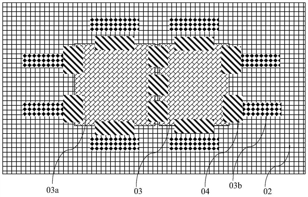
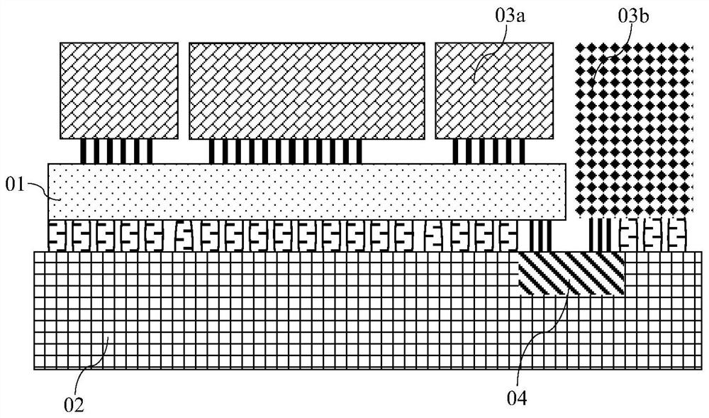
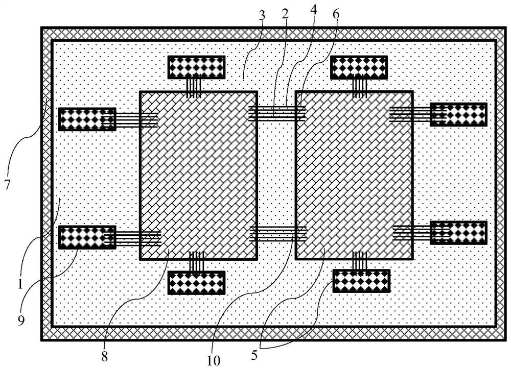
[0063] refer to Figure 2A and Figure 2B As shown, the packaged device of the high-density interconnection system provided by the present invention includes: a high-density wire-planted circuit board 1, which is implanted into a prepreg 3 by using a wire 2 and then heated and pressurized so that the glue of the prepreg is cured to form a high-density wire-planted circuit board 1. The wire 2 has a terminal 4. The chip 5 is arranged on the high-density wiring circuit board 1, and the connecting pin 6 of the chip is connected with the terminal 4 of the wire.

[0064] The line width of the outline dimension of the wire is less than or equal to 2 μm, and the minimum value of the line distance between two adjacent wires can be less than or equal to 2 μm. The meaning of the line width of the outline dimension is the diameter of the circle that co...


PUM


Abstract

The invention discloses a high-density interconnection system packaging device which comprises a high-density embedded wire circuit board which is formed by embedding a wire into a prepreg and then carrying out heating and pressurization to enable a glue solution of the prepreg to be cured so as to form the high-density embedded wire circuit board, and the wire is provided with a wiring end; and the device also comprises a chip which is arranged on the high-density embedded wire circuit board, and a connecting pin of the chip is connected with the wiring end of the wire. The manufacturing method of the high-density interconnection system packaging device comprises the steps that the wire is implanted into the prepreg, then heating and pressurizing are carried out, so that a glue solution of the prepreg is cured to form the high-density embedded wire circuit board, and the wire forms a wiring end; the chip is arranged on the high-density embedded wire circuit board, and the connecting pin of the chip is connected with the wiring end of the wire. Therefore, the wire width and the wire distance of the wire layer on the high-density embedded wire circuit board are 1-2 microns, the wiring density is increased, and the communication density between chips is increased; due to the increase of the density of the wires, the arrangement quantity of the chips is increased, the size of the packaging bag is reduced, and more information transmission and data communication are realized.

Description

technical field [0001] The invention relates to the field of semiconductor products, in particular to a high-density interconnection system packaging device. [0002] The present invention relates to the field of semiconductor manufacturing methods, in particular to a manufacturing method of high-density interconnection system packaging devices. Background technique [0003] The 21st century is the information age, and the information industry is an important force to promote the continuous progress of human society. The modern information industry covers many manufacturing fields, among which chip manufacturing, electronic packaging and product testing are all essential production processes. Electronic packaging is a multidisciplinary high-tech industry, involving machinery, electronics, materials, physics, chemistry, optics, mechanics, heat, electromagnetics, communication, computer, control and other disciplines, and has become one of the key areas for the development of...

Claims


Application Information

Patent Timeline
IPC IPC(8): H01L23/488H01L25/18H01L21/60H05K1/18H05K3/46H05K3/34
CPCH01L24/24H01L24/85H01L25/18H05K1/181H05K3/4658H05K3/3426H01L2224/24226
Inventor 贺江奇孙贵宝袁强洪丹红贺健程浩
Owner 宁波甬强科技有限公司
Why Eureka
Try Eureka