

Level conversion circuit
a level conversion and circuit technology, applied in the direction of logic circuit coupling/interface arrangement, pulse generator, pulse technique, etc., can solve the problems of long delay time of the level conversion circuit and slow circuit operation speed, so as to prevent a decrease in the operation speed and reduce the power supply voltage
- Summary
- Abstract
- Description
- Claims
- Application Information
AI Technical Summary
Benefits of technology
Problems solved by technology
Method used
Image

Examples
first embodiment
[0084] (First Embodiment)
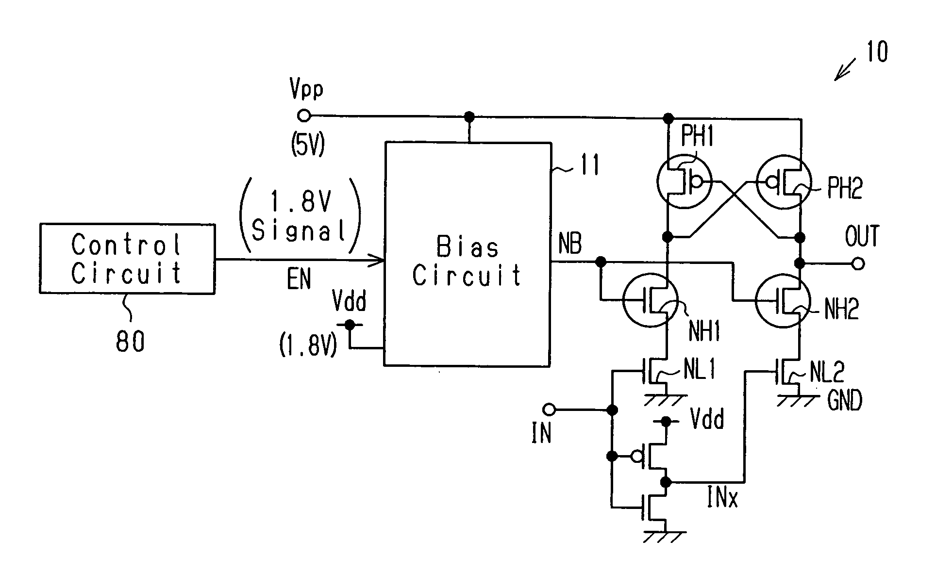
[0085] The following describes a level conversion circuit 10 according to a first embodiment of the present invention.
[0086]FIG. 7 shows the level conversion circuit 10 according to the first embodiment. The level conversion circuit 10 includes a bias circuit 11 for generating a bias potential NB. The bias circuit 11 differs from the corresponding component of the conventional example shown in FIG. 2. In FIG. 7, components that are the same as the corresponding components of the conventional example in FIG. 2 (the MOS transistors PH1, PH2, NH1, and NH2, the inverter circuits 3 and 4, etc.,) are given the same reference numerals as those components.
[0087] The level conversion circuit 10 converts an input signal IN, which has a signal level that oscillates between a reference voltage of 0 V and a power supply voltage Vdd of 1.8 V, into an output signal OUT, which has a signal level that oscillates between the reference voltage GND of 0 V and a second power s...
second embodiment
[0116] (Second Embodiment)
[0117] An AD conversion circuit 15 according to a second embodiment of the present invention will now be described with reference to the drawings.
[0118]FIG. 8 shows the AD conversion circuit 15, which includes the level conversion circuit 10 of the first embodiment.
[0119] The AD conversion circuit 15 according to the second embodiment is a sequential comparison AD conversion circuit for converting an analog signal Vin into a 4-bit digital signal. The AD conversion circuit 15 is used, for example, in a semiconductor integrated circuit device (LSI) for automobiles. The AD conversion circuit 15 includes, in addition to the level conversion circuit 10, first and second switch circuits SW1 and SW2, sampling capacitors CS1, CS2, CS3, CS4, and CS5, a comparator 16, a level conversion circuit 17, and a sequential comparison control circuit 18.
[0120] Capacitance values of the sampling capacitors CS1 to CS5 are binary-weighted values. The capacitor values are set ...
third embodiment
[0142] (Third Embodiment)
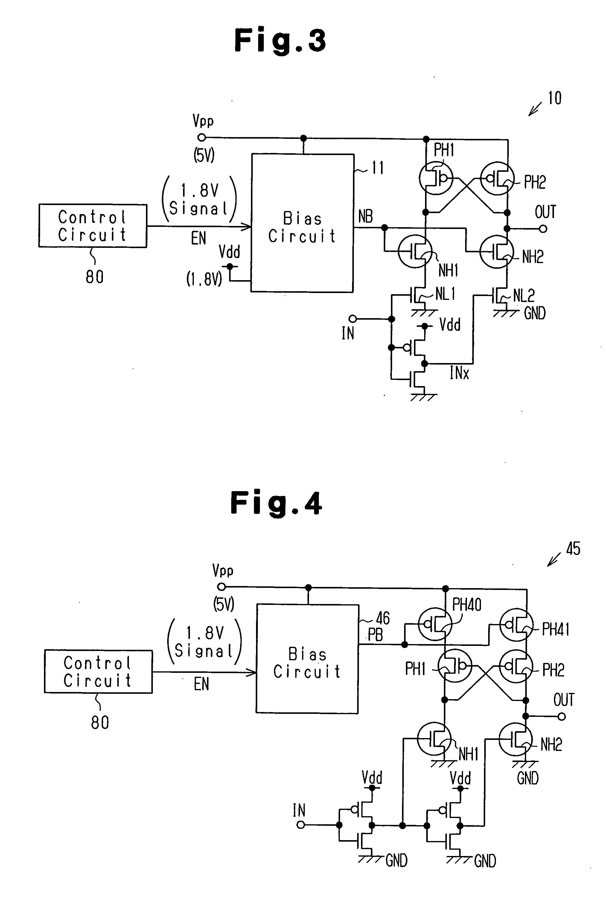
[0143] The following describes a level conversion circuit 22 according to a third embodiment of the present invention.
[0144]FIG. 12 shows the level conversion circuit 22 according to the third embodiment. The level conversion circuit 22 differs from the level conversion circuit 10 of the first embodiment in that its bias circuit 23 has a circuit structure differing from the corresponding component, and the level conversion circuit 22 additionally includes an inverter circuit 24 formed by a low voltage capacity PMOS transistor PL3 and a low voltage capacity NMOS transistor NL3. In FIG. 12, components that are the same as the corresponding components in the first embodiment (refer to FIG. 7) are given the same reference numerals as those components. The following describes the third embodiment focusing on its differences from the first embodiment.
[0145] The potential at the output node N10 of the inverter circuit 3 shifts from a H level to a L level when a c...
PUM
 Abstract
Description
Claims
Application Information