Thin film circuit substrate, piezoelectric speaker device, display device, and sound-generating display device

a display device and thin film circuit technology, applied in the direction of emergency protective arrangements for limiting excess voltage/current, identification means, instruments, etc., can solve the problems of no measures taken against surge voltage and current, damage to the drive circuit of the voice-output section on the thin film circuit substrate, damage to the display-section drive circuit, etc., to prevent damage to the circuit section, easy to form, and small the effect of an entire devi

Inactive Publication Date: 2005-10-27
SHARP KK
View PDF14 Cites 31 Cited by
  • Summary
  • Abstract
  • Description
  • Claims
  • Application Information

AI Technical Summary

Benefits of technology

[0014] In such an arrangement, an antisurge element, provided on a wiring between a circuit section and an input terminal section thereof or an output terminal section thereof, removes an excess charge from the wiring by bypassing the wiring to the ground when a voltage applied to the wiring exceeds beyond a predetermined range. This makes it possible to protect a drive circuit by preventing damage to the circuit section caused by a current (surge current), generated by an excess voltag...

Problems solved by technology

However, in a piezoelectric speaker device and a display device which include a conventional drive circuit constituted of a thin film circuit substrate, as well as in the arrangement described in Document 1, no measures are taken against a surge voltage and current.
This might cause damage to the voice-output-section drive circuit on the thin film circuit substrate.
This might cause damage to the display-section drive circuit.
However, since the thin film circuit substrate, presupposed by the present invention, which constitutes a drive circuit of a thin film layer, uses not a bonded-type but a MOS-FET thin film, PN bonding becomes difficult.
Therefore, under the existing circ...

Method used


Image

  • Thin film circuit substrate, piezoelectric speaker device, display device, and sound-generating display device
  • Thin film circuit substrate, piezoelectric speaker device, display device, and sound-generating display device
  • Thin film circuit substrate, piezoelectric speaker device, display device, and sound-generating display device

Examples


first embodiment

[0036] [First Embodiment]

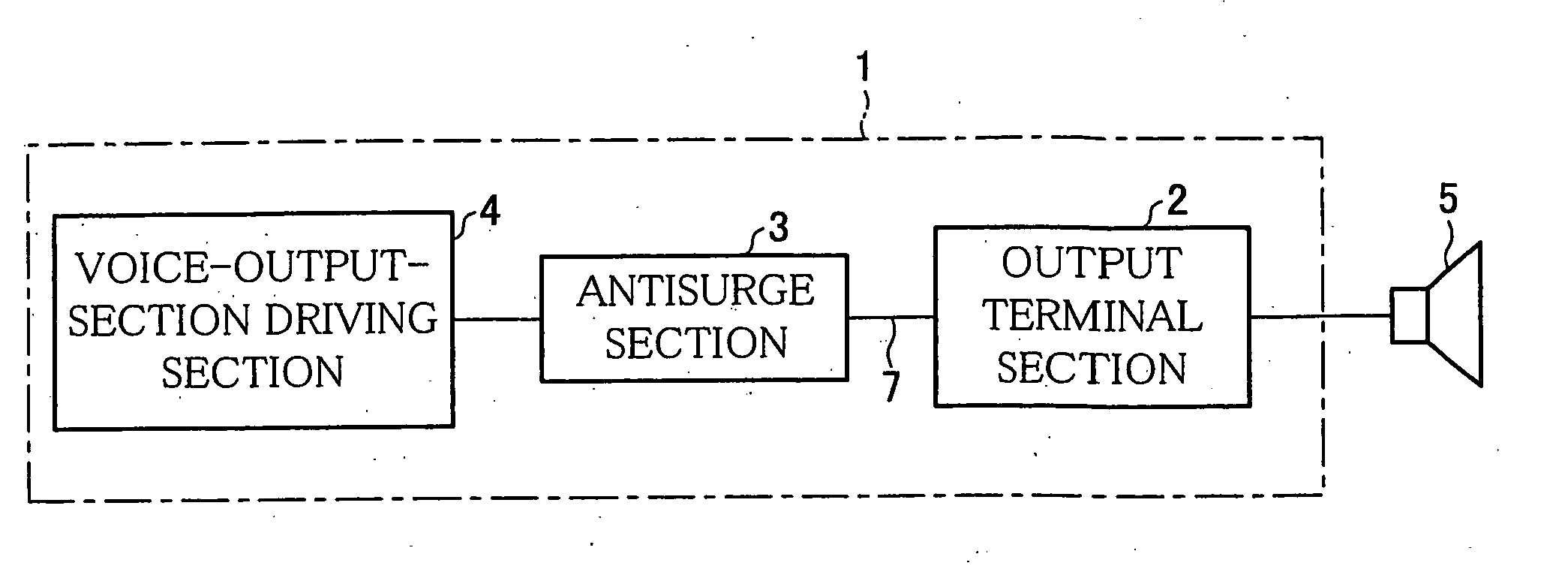
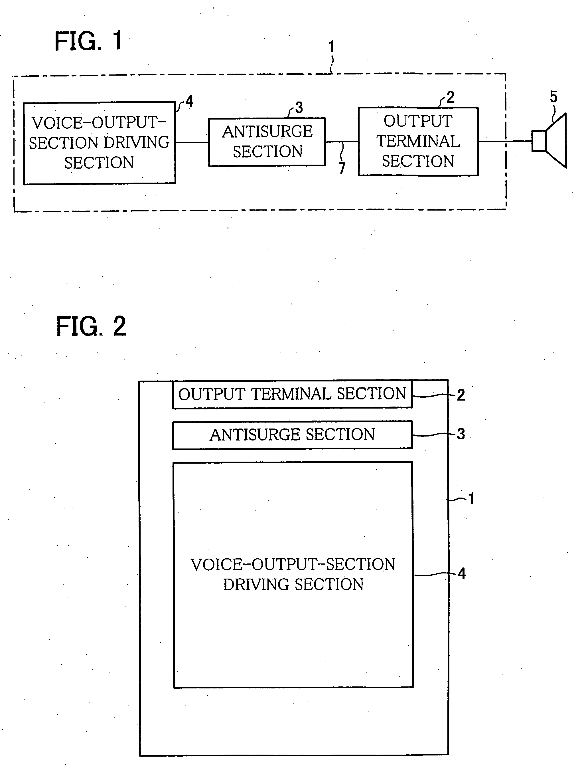
[0037]FIG. 1 is a functional block diagram showing a thin film circuit substrate 1, constituting a drive circuit of a piezoelectric speaker device, according to one embodiment of the present invention. FIG. 2 is a diagram showing a configuration of components on the thin film circuit substrate 1.

[0038] As shown in FIGS. 1 and 2, the thin film circuit substrate 1 is provided with an output terminal section 2, an antisurge section 3, and a voice-output-section actuator 4. The thin film circuit substrate 1 includes an insulative substrate (e.g. glass) and a thin film layer, having a polycrystalline silicon thin film, which is formed thereon. The voice-output-section driving section 4 is monolithically formed of the thin film layer. The voice-output-section driving section 4, constituted of a thin film element (e.g. a thin film transistor) formed of the thin film layer, converts an incoming audio signal into an drive signal for driving a voice output section 5,...

second embodiment

[0058] [Second Embodiment]

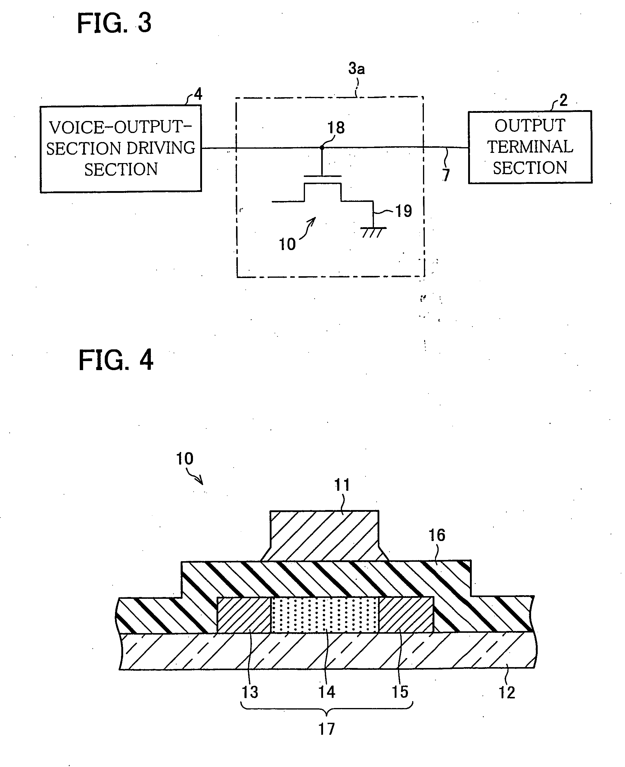
[0059] In the following, a thin film circuit substrate according to another embodiment of the present invention will be described in reference to FIG. 6. The thin film circuit substrate is a thin film circuit substrate which constitutes a drive circuit of a piezoelectric speaker device, and is different only in an arrangement of an antisurge element from the thin film circuit substrate according to the First Embodiment. Therefore, only the arrangement of the antisurge element is described here.

[0060] When a high-frequency characteristic is not expected judging from a frequency characteristic of a load piezoelectric element serving as a voice output section 5, it is preferable, as shown in FIG. 6, that an antisurge element include a voltage damper utilizing source-grounded operation of a thin film transistor.

[0061] An antisurge element 3c shown in FIG. 6 is provided with a source-grounded MOS transistor (second MOS transistor) 53, whose gate terminal is co...

third embodiment

[0068] [Third Embodiment]

[0069] In the following, a thin film circuit substrate 20, constituting a drive circuit of a display device, according to a further embodiment of the present invention will be described in reference to FIGS. 7 and 8. FIG. 7 is a functional block diagram showing an arrangement of the thin film circuit substrate 20. FIG. 8 is a diagram showing a configuration of components on the thin film circuit substrate 20. It is to be noted, for the sake of convenience in description, that the same reference mark is appended to a component having the same function as in the First Embodiment. Description of the component is omitted.

[0070] As shown in FIGS. 7 and 8, the thin film circuit substrate 20 is provided with a display driving section (display driving circuit) 22, a display section 23, an antisurge section 3, and an input terminal section 21. The display driving section 22 is constituted of a video-signal input section 26, a signal-line driver 27, and a scanning-li...


PUM


Abstract

A thin film circuit substrate is provided with a voice-output-section driving section, formed of a thin film layer on an insulative substrate, for driving a voice output section. An antisurge section, provided on a wiring between the voice-output-section driving section and an output terminal section thereof, includes an antisurge element. When a surge voltage is applied to the wiring, the antisurge element, monolithically formed on the thin film circuit substrate, connects the wiring to the ground so as to pass a current (surge current), generated by the surge voltage applied to the wiring, to the ground. This makes it possible to provide a thin film circuit substrate which is monolithically provided with a function which can protect a circuit section when a voltage exceeding a predetermined range is applied to the wiring linking the circuit section with an input terminal section or an output terminal section.

Description

[0001] This Nonprovisional application claims priority under 35 U.S.C. § 119(a) on Patent Application No. 127020 / 2004 filed in Japan on Apr. 22, 2004, the entire contents of which are hereby incorporated by reference. FIELD OF THE INVENTION [0002] The present invention relates to a thin film circuit substrate including a circuit section, such as a drive circuit, constituted of a thin film layer formed on an insulative substrate, such as a glass substrate, and a piezoelectric speaker device and a display device provided with the same. BACKGROUND OF THE INVENTION [0003] Conventionally, a piezoelectric speaker device has been used which outputs a voice by causing an excitation source section constituted of an piezoelectric element to vibrate a vibration section (e.g., a diaphragm) based on an audio signal. In addition, a compact, lightweight, thin display element has appeared recently. There has been commercialized a portable display device, with such a display element, capable of capt...

Claims


Application Information

Patent Timeline
IPC IPC(8): G02F1/1362H04R17/00G09F9/00H01L21/02H01L21/336H01L21/822H01L27/04H01L27/06H01L27/08H01L27/12H01L29/786H02H9/00H04R3/00H04R23/00
CPCG02F1/1362G09G2330/04H04R2400/00H04R17/00H04R3/007H01L27/01
Inventor MIYATA, KAZUHIKO
Owner SHARP KK
Why Eureka
Try Eureka