
Electrically erasable charge trap nonvolatile memory cells having erase threshold voltage that is higher than an initial threshold voltage

a charge trap and non-volatile memory technology, applied in semiconductor devices, digital storage, instruments, etc., can solve the problems of deteriorating the endurance and/or speed losing all stored data, etc., and reducing the erasing time. , the endurance of electrically erasable charge trap non-volatile memory cells is determined.

Inactive Publication Date: 2005-10-27
SAMSUNG ELECTRONICS CO LTD
View PDF45 Cites 7 Cited by
  • Summary
  • Abstract
  • Description
  • Claims
  • Application Information

AI Technical Summary

Benefits of technology

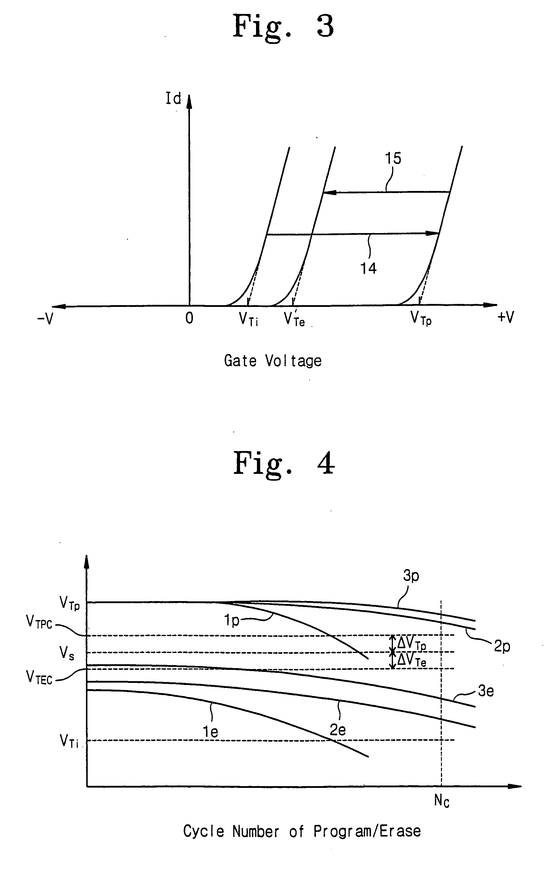
The present invention provides an electrically erasable charge trap nonvolatile memory cell with a higher erase threshold voltage compared to the initial threshold voltage. This allows for faster erasing compared to conventional memory cells, which may increase the endurance of the memory cell. The method of erasing the memory cell involves applying an erase voltage for a time interval that lowers the threshold voltage of the transistor from a program threshold voltage to the erase threshold voltage. The time interval is determined based on an endurance specification for the memory cell, which includes a critical erase threshold voltage, a critical program threshold voltage, and a critical number of erase / program cycle operations for the memory cell. The endurance test is performed repeatedly using a time interval that is increased or decreased from the initial time interval, to obtain the time interval that meets the endurance specification. The invention also attempts to successfully read the memory cell using increased or decreased time intervals after performing an endurance test.

Problems solved by technology

These volatile memory devices lose their data when their power supplies are interrupted.
Since the floating gate device stores charges as free carriers, all stored data may be lost if a tunnel oxide layer thereof is even partially defective.
It is well known that the erase operation can impact the endurance of the electrically erasable charge trap nonvolatile memory cell by attacking the interface between the substrate and the tunnel insulating layer during the erase operation, which may create interface traps.
These interface traps may deteriorate the endurance and / or speed of an electrically erasable charge trap nonvolatile memory cell.

Method used


Image

  • Electrically erasable charge trap nonvolatile memory cells having erase threshold voltage that is higher than an initial threshold voltage
  • Electrically erasable charge trap nonvolatile memory cells having erase threshold voltage that is higher than an initial threshold voltage
  • Electrically erasable charge trap nonvolatile memory cells having erase threshold voltage that is higher than an initial threshold voltage

Examples


Embodiment Construction

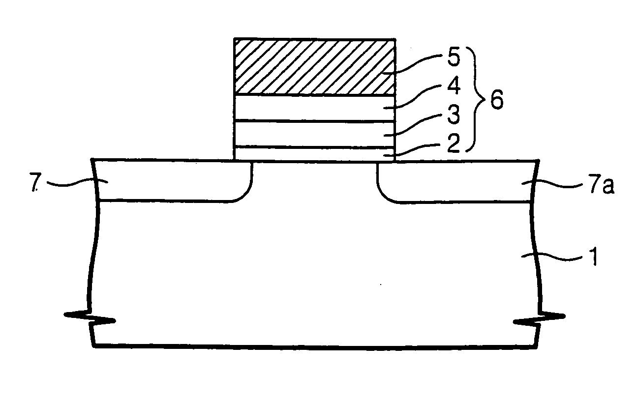
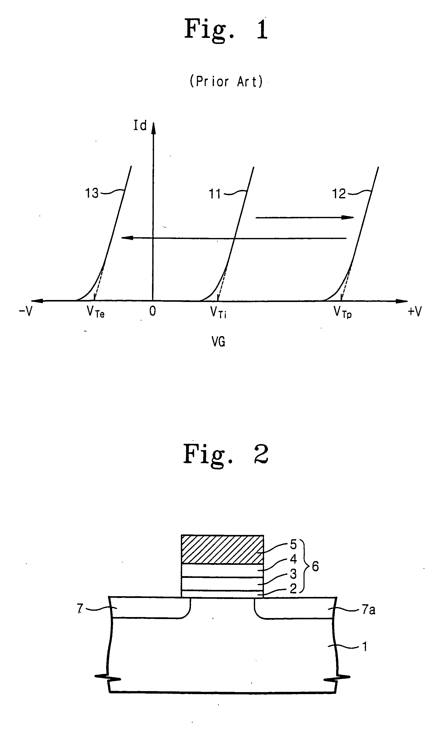
[0020] The present invention now will be described more fully hereinafter with reference to the accompanying drawings, in which embodiments of the invention are shown. However, this invention should not be construed as limited to the embodiments set forth herein. Rather, these embodiments are provided so that this disclosure will be thorough and complete, and will fully convey the scope of the invention to those skilled in the art. In the drawings, the thickness of layers and regions are exaggerated for clarity. Like numbers refer to like elements throughout. It will be understood that when an element such as a layer, region or substrate is referred to as being “on” or extending “onto” another element, it can be directly on or extend directly onto the other element or intervening elements may also be present. In contrast, when an element is referred to as being “directly on” or extending “directly onto” another element, there are no intervening elements present. Moreover, each embod...


PUM


Abstract

An electrically erasable charge trap nonvolatile memory cell has an initial threshold voltage, a program voltage that is higher than the initial threshold voltage, and an erase threshold voltage that is lower than the program threshold voltage but is higher than the initial threshold voltage. The programmed electrically erasable charge trap nonvolatile memory cells may be erased by applying an erase voltage for a time interval that is sufficient to lower the threshold voltage the transistor from a program threshold voltage to an erase threshold voltage that is lower than the program threshold voltage, but is higher than the initial threshold voltage. The time interval may be determined by repeatedly performing an endurance test using a time interval that is increased or decreased from an initial time interval, to obtain the time interval that meets an endurance specification, or allows a read to be performed successfully.

Description

RELATED APPLICATIONS [0001] This application is a continuation of application Ser. No. 10 / 401,372, filed Mar. 28, 2003, entitled Electrically Erasable Charge Trap Nonvolatile Memory Cells Having Erase Threshold Voltage That is Higher Than an Initial Threshold Voltage, and claims the benefit of Korean Patent Application No. 2002-0025195, filed May 8, 2002, the disclosures of which are hereby incorporated herein by reference in their entirety as if set forth fully herein.FIELD OF THE INVENTION [0002] This invention relates to nonvolatile memory devices, and more particularly to electrically erasable charge trap nonvolatile memory devices. BACKGROUND OF THE INVENTION [0003] Integrated circuit memory devices are widely used in consumer and commercial applications. As is well known to those having skill in the art, integrated circuit memory devices include volatile and nonvolatile memory devices. Volatile memory devices may include Dynamic Random Access Memory (DRAM) devices and Static R...

Claims


Application Information

Patent Timeline
Patent Type & Authority Applications(United States)
IPC IPC(8): H10B69/00G11C16/04G11C16/14H01L29/792
CPCG11C16/04G11C16/0466G11C16/10G11C29/50004G11C16/349G11C29/50G11C16/14H01L29/792H10B69/00
Inventor LEE, CHANG-HYUN
Owner SAMSUNG ELECTRONICS CO LTD
Learn More