Method for producing micromechanical and micro-optic components consisting of glass-type materials

a technology of glass-type materials and micro-optic components, which is applied in the direction of glass shaping apparatus, electrostatic generators/motors, cameras, etc., can solve the problems of poor surface quality, strong restriction of precision and shape variation, and limited lateral dimension, so as to achieve precise and low-cost shaping of elements

a technology of glass-type materials and micro-optic components, which is applied in the direction of glass shaping apparatus, electrostatic generators/motors, cameras, etc., can solve the problems of poor surface quality, strong restriction of precision and shape variation, and limited lateral dimension, so as to achieve precise and low-cost shaping of elements

US20050239228A1Inactive Publication Date: 2005-10-27FRAUNHOFER GESELLSCHAFT ZUR FOERDERUNG DER ANGEWANDTEN FORSCHUNG EV

Image

  • Method for producing micromechanical and micro-optic components consisting of glass-type materials
  • Method for producing micromechanical and micro-optic components consisting of glass-type materials
  • Method for producing micromechanical and micro-optic components consisting of glass-type materials

Examples


Embodiment Construction

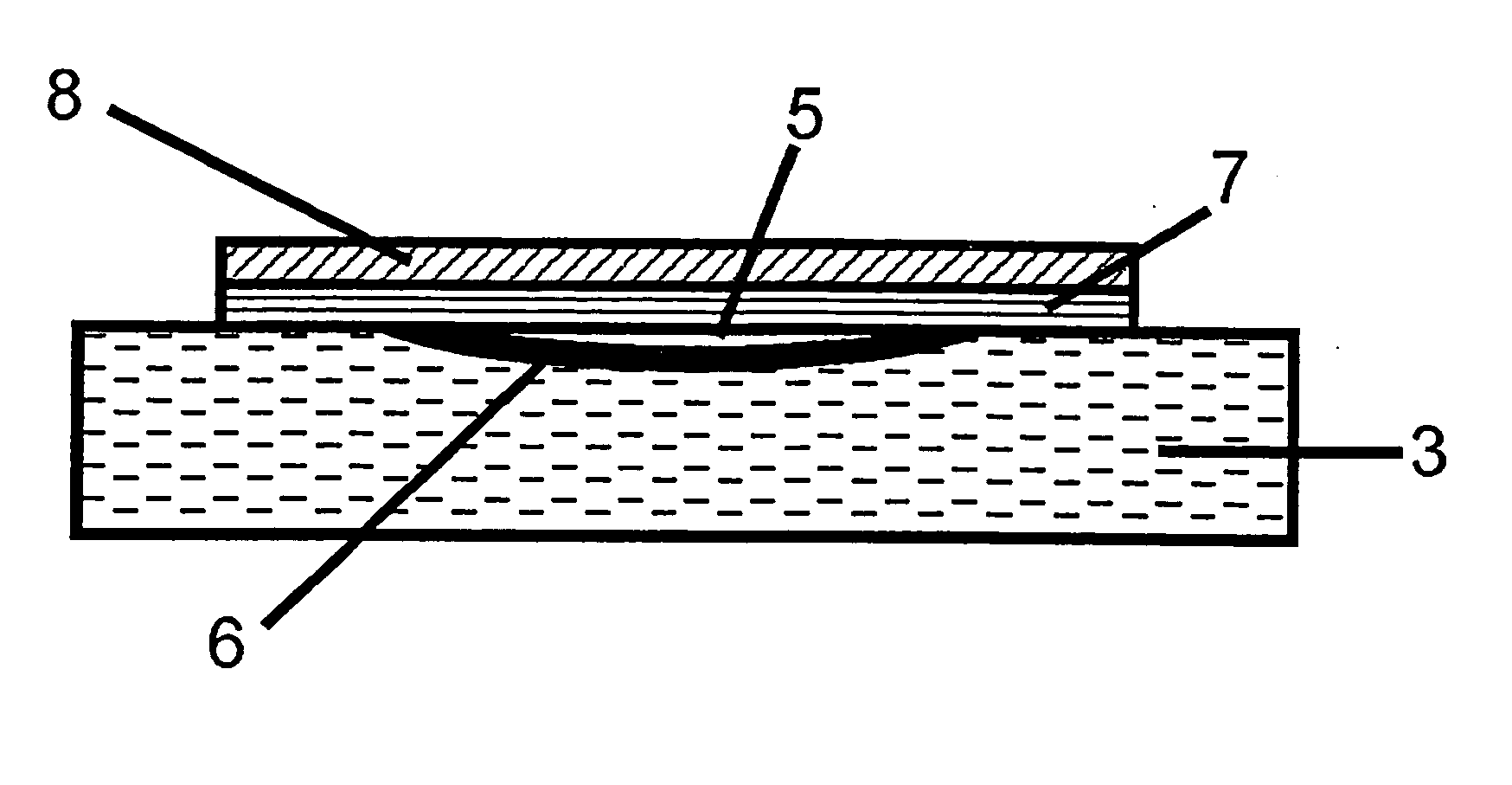
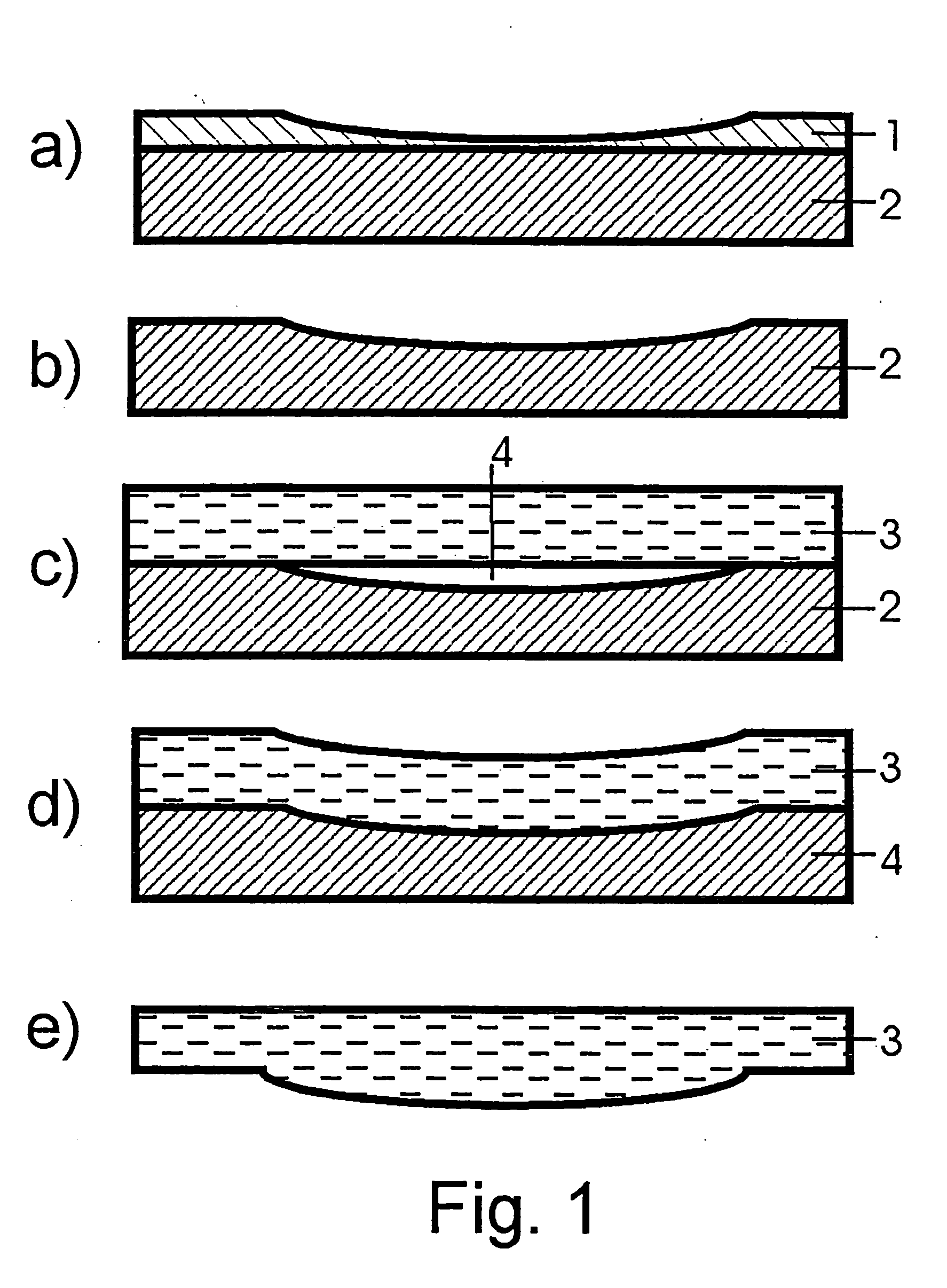
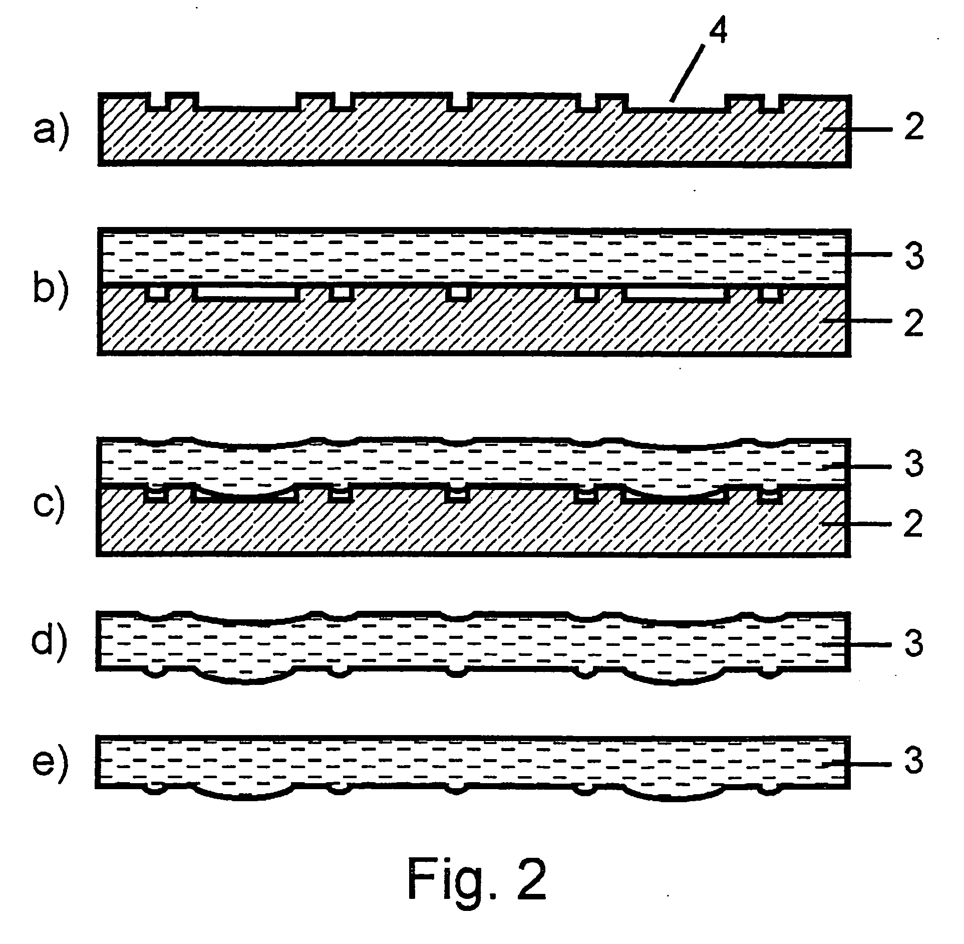
[0040]FIG. 1 illustrates various stages of a process for the manufacture of a micro-structure glass surface with application of the inventive method for projecting a structured silicon surface. These are manufacturing stages following the completion of the following operating steps: [0041] (a) formation of a structure in the photo resist (1), [0042] (b) transfer of the structure by etching the photo resist and the surface of the silicon wafer (2), [0043] (c) anodic bonding of a Pyrex® glass wafer (3) onto the silicon surface structure with recesses (4), preferably under conditions resembling a vacuum, [0044] (d) annealing and inflow of the glass into the silicon surface structures under the action of overpressure and / or required by the difference in pressure between the furnace atmosphere and the pressure situation created in the anodic bonding process and preserved in the silicon surface recesses, [0045] (e) grinding and polishing the glass surface turned away from the silicon, aft...


PUM

PropertyMeasurementUnit
wavelengthsaaaaaaaaaa
sizeaaaaaaaaaa

Abstract

What is proposed here is a method of structuring surfaces of glass-type materials and variants of this method, comprising the following steps of operation: providing a semiconductor substrate, structuring, with the formation of recesses, of at least one surface of the semiconductor substrate, providing a substrate of glass-type material, joining the semiconductor substrate to the glass-type substrate, with a structured surface of the semiconductor substrate being joined to a surface of the glass-type surface in an at least partly overlapping relationship, and heating the substrates so bonded by annealing in a way so as to induce an inflow of the glass-type material into the recesses of the structured surface of the semiconductor substrate. The variants of the method are particularly well suitable for the manufacture of micro-optical lenses and micro-mechanical components such as micro-relays or micro-valves.

Description

[0001] The present invention relates to a method of producing micro-mechanical and micro-optic components and / or functional elements consisting of glass-type materials, which permits the duplication modelling of structured substrate surfaces in glass, with utilisation of the flow properties of the glass and with application of standard methods in semiconductor technology. The term “functional element” is meant to denote a substrate with a structured surface in accordance with the present invention, which consists of glass-type material and is used in further-going steps of method. [0002] Shaping methods, e.g. in mono-crystalline silicon, are widely common as standard methods in semiconductor technology. For transmissive micro-optical components such as lenses, optical gratings or beam shapers, however, semiconductor materials are suitable only conditionally. Silicon, for instance, presents a strong absorption in the visible range of wavelengths of the light. Optical components for w...

Claims


Application Information

Patent Timeline
27 Oct 2005
Publication
US20050239228A1
IPC
B81B7/00; G02B3/00; C03B11/00; C03B11/08; C03B23/02; C03B23/025; C03B23/203; C03C19/00; G03B7/00; H02N1/00
CPC
B81B2201/018; B81B2201/047; B81C1/00047; B81C99/008; B81C99/0085; C03B2215/412; C03B23/0252; C03B23/203
Inventors
QUENZER, HANS-JOACHIM; MERZ, PETER