Lithographic apparatus and device manufacturing method

Active Publication Date: 2005-11-03
ASML NETHERLANDS BV
View PDF4 Cites 13 Cited by
  • Summary
  • Abstract
  • Description
  • Claims
  • Application Information

AI Technical Summary

Benefits of technology

[0007] It is an aspect of the present invention to provide a lithographic apparatus including a simple and cost-eff

Problems solved by technology

SR (synchrotron radiation) sources have been investigated as EUV radiation sources, but their output power is insufficient for use in EUV lithography.
In addition, they are relatively large and expensive which makes them unattractive for practical applications.
The achievable output power of the DP EUV sources is limited by the heat load of the system, which is dominated by three heating effects.
First, the combination of the large electrical current that passes through the plasma and the electrodes and the non-zero electrical resistance of the electrodes

Method used


Image

  • Lithographic apparatus and device manufacturing method
  • Lithographic apparatus and device manufacturing method
  • Lithographic apparatus and device manufacturing method

Examples


Embodiment Construction

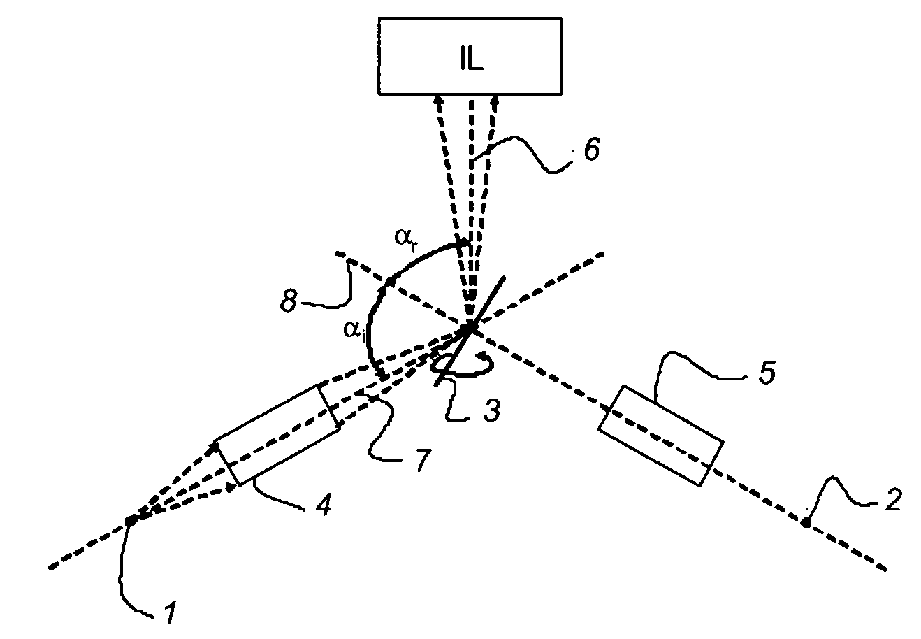
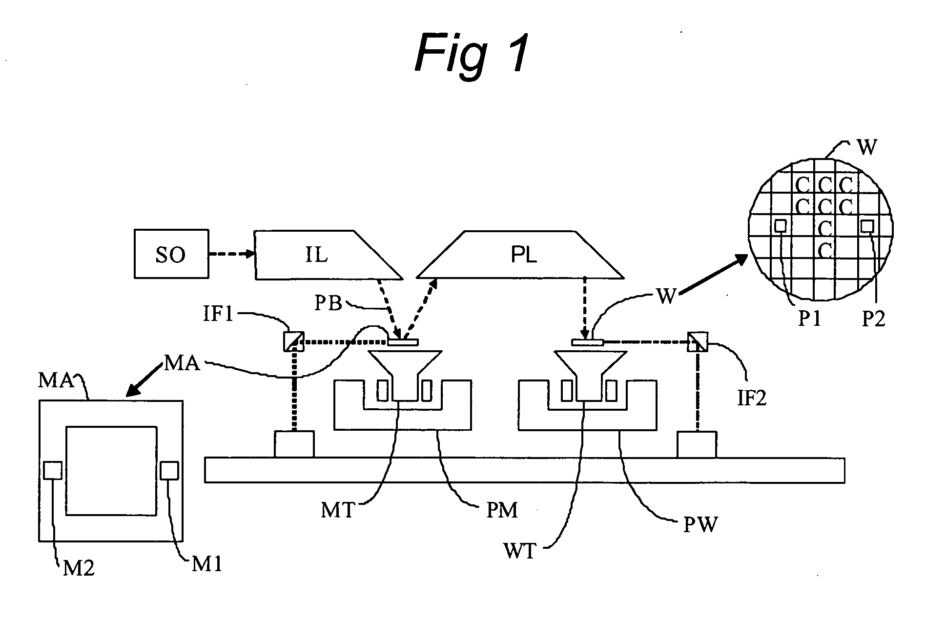
[0039]FIG. 1 schematically depicts a lithographic apparatus according to an exemplary embodiment of the present invention, including an illumination system (illuminator) IL configured to provide a beam PB of radiation (e.g. UV or EUV radiation). A first support structure (e.g. a mask table) MT is configured to support a patterning device (e.g. a mask) MA and is connected to first positioning device PM that accurately positions the patterning device with respect to a projection system (“lens”) PL. A substrate table (e.g. a wafer table) WT is configured to hold a substrate (e.g. a resist-coated wafer) W and is connected to a second positioning device PW that accurately positions the substrate with respect to the projection system PL. The projection system (e.g. a reflective projection lens) PL is configured to image a pattern imparted to the beam PB by the patterning device MA onto a target portion C (e.g. including one or more dies) of the substrate W.

[0040] As here depicted, the ap...


PUM


Abstract

A lithographic apparatus includes an illumination system configured to provide a beam of radiation, a support configured to support a patterning device, a substrate table and a projection system. Furthermore, the lithographic apparatus includes a plurality of EUV sources for providing EUV radiation to the illumination system and distribution means which are arranged to convert the EUV radiation from each of the EUV sources into an intermediate beam of radiation. The intermediate beam of radiation is directed from the distribution means in a first direction by a mirror surface. The distribution means further comprise a rotationally driven mirror arrangement, the axis of rotation being non-parallel to the mirror surface.

Description

BACKGROUND OF THE INVENTION [0001] 1. Field of the Invention [0002] The present invention relates to a lithographic apparatus and a device manufacturing method. [0003] 2. Description of the Related Art [0004] A lithographic apparatus is a machine that applies a desired pattern onto a target portion of a substrate. Lithographic apparatus can be used, for example, in the manufacture of integrated circuits (ICs). In that circumstance, a patterning device, such as a mask, may be used to generate a circuit pattern corresponding to an individual layer of the IC, and this pattern can be imaged onto a target portion (e.g. including part of one or several dies) on a substrate (e.g. a silicon wafer) that has a layer of radiation-sensitive material (resist). In general, a single substrate will contain a network of adjacent target portions that are successively exposed. Known lithographic apparatus include so-called steppers, in which each target portion is irradiated by exposing an entire patt...

Claims


Application Information

Patent Timeline
IPC IPC(8): G02B5/08G03B27/54G03F7/20H01L21/027
CPCG03F7/7005G03F7/70008
Inventor BANINE, VADIM YEVGENYEVICHBAKKER, LEVINUS PIETERJONKERS, JEROENLOOPSTRA, ERIK ROELOF
Owner ASML NETHERLANDS BV
Why Eureka
Try Eureka