Nonvolatile semiconductor memory device that achieves speedup in read operation

Inactive Publication Date: 2005-11-03
RENESAS ELECTRONICS CORP
View PDF5 Cites 6 Cited by
  • Summary
  • Abstract
  • Description
  • Claims
  • Application Information

AI Technical Summary

Benefits of technology

[0010] It is an object of the present invention to provide a nonvolatile semiconductor memory device that achieves speedup in read o

Problems solved by technology

The nonvolatile semiconductor memory device disclosed in JP 11-191298, however, requires the same number of control signal lines for the first transistor and the second transistor, putting restrictions on wiring in terms of layout.
This poses a first problem of a

Method used


Image

  • Nonvolatile semiconductor memory device that achieves speedup in read operation
  • Nonvolatile semiconductor memory device that achieves speedup in read operation
  • Nonvolatile semiconductor memory device that achieves speedup in read operation

Examples


first preferred embodiment

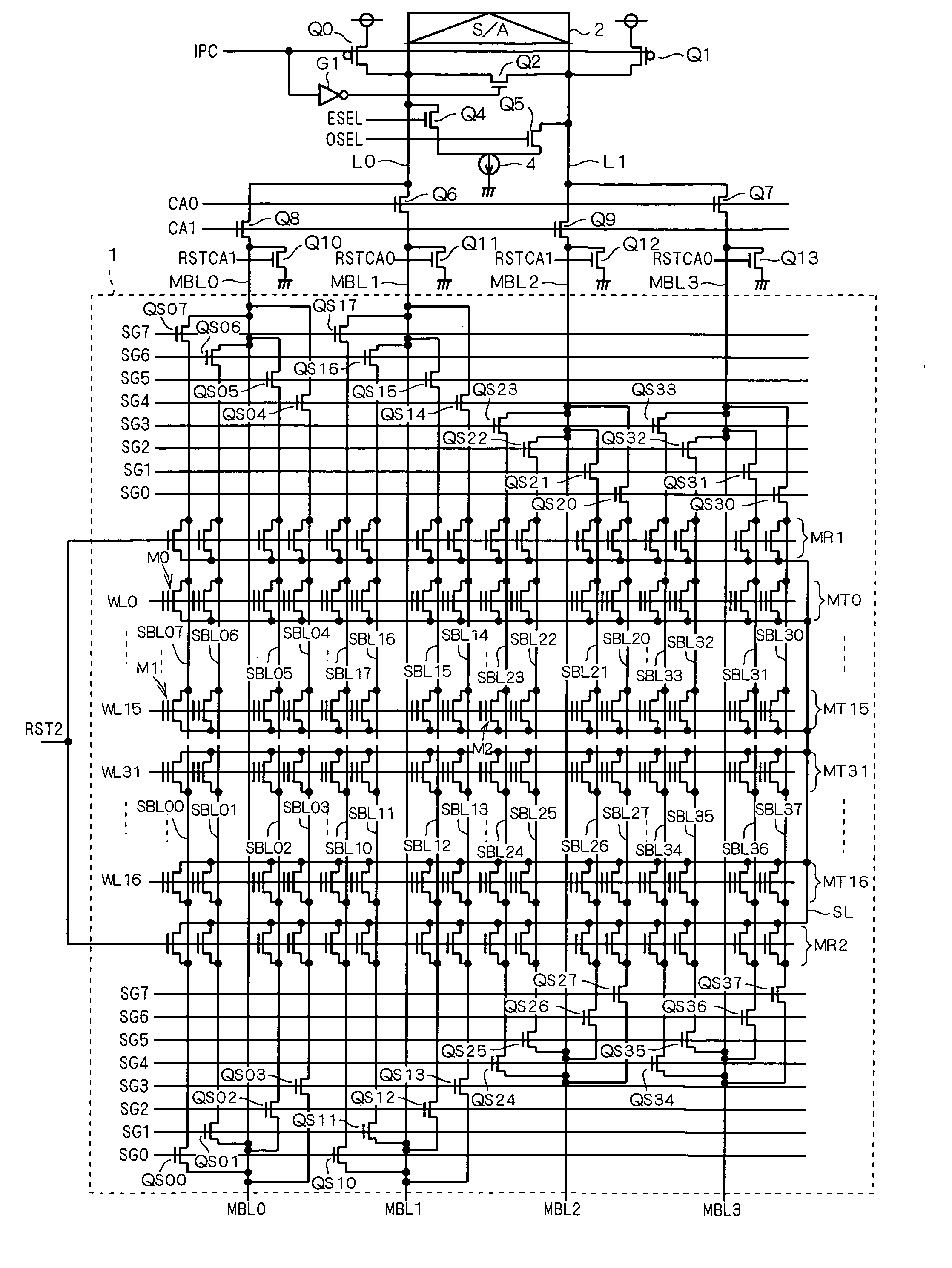
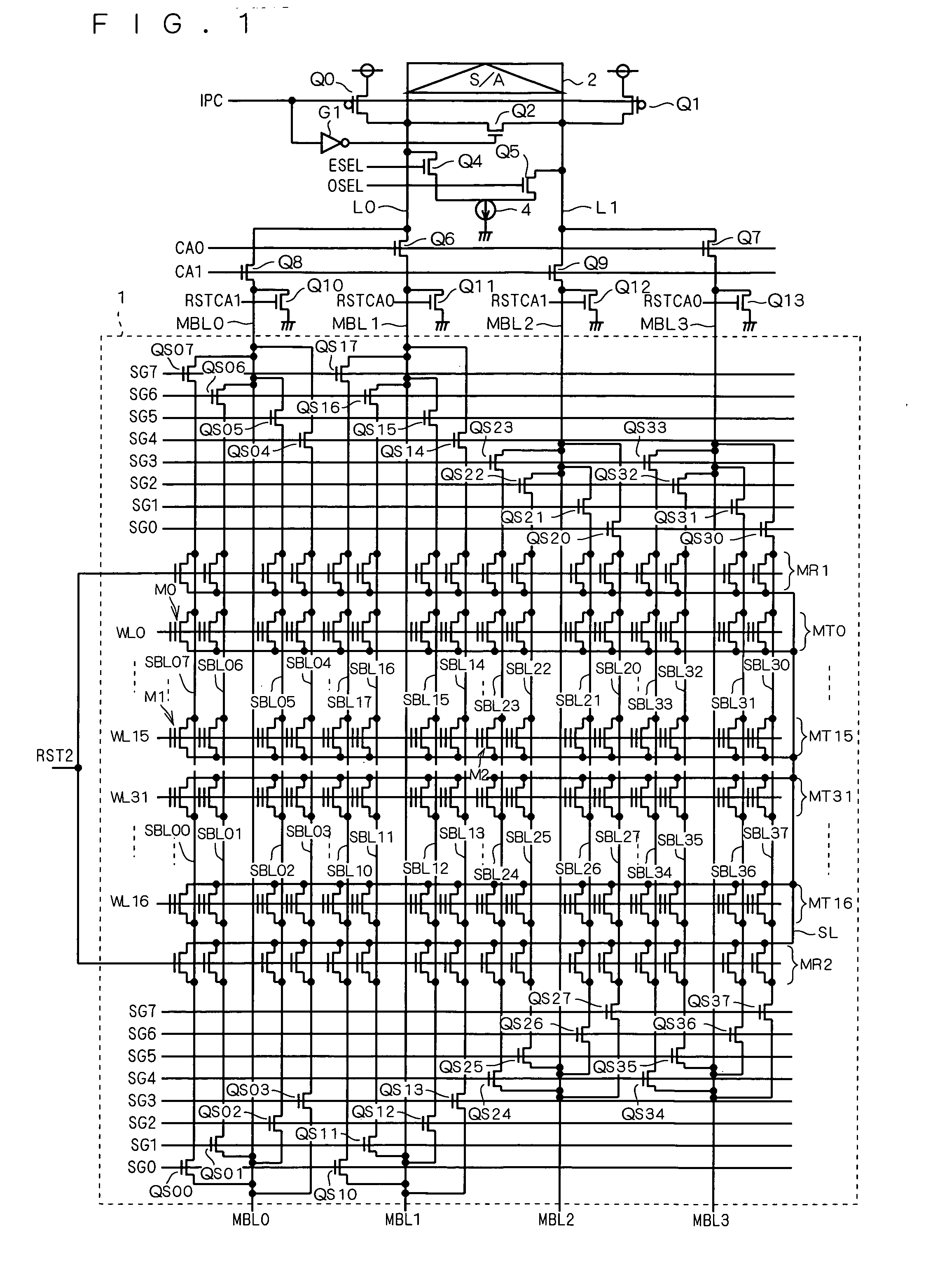
[0026]FIG. 1 is a circuit diagram illustrating part of a read circuit configuration in a flash memory according to a first preferred embodiment of the present invention. As shown, an erase block 1 is provided correspondingly to one sense amplifier 2. In actuality, a plurality of erase blocks provided correspondingly to a plurality of sense amplifiers constitute a group of erase blocks erasable at a time. For example, to 64 sense amplifiers, 64 erase blocks 1 shown in FIG. 1 may constitute a group of erase blocks of one unit, or 32 sense amplifiers each may constitute a group of erase blocks of two units. Alternatively, a predetermined number of erase blocks 1 shown in FIG. 1 may be further provided in the direction of main bit line.

[0027] The sense amplifier 2 is a differential circuit supporting high-speed reading that obtains read data by detecting and amplifying a difference between the amounts of current flowing through sense lines L0 and L1, respectively. Precharge transistors...

second preferred embodiment

[0067]FIG. 6 is a circuit diagram illustrating part of a read circuit configuration in a flash memory according to a second preferred embodiment of the present invention. As shown, inversion buffers 5 and 7 having their respective inputs receiving the sub-bit line reset signal RST2 are provided, and inversion buffers 5 and 6 connected in series output an upper sub-bit line reset signal URSTSBL to the gates of the sub-bit line reset transistors MR1, while inversion buffers 7 and 8 connected in series output a lower sub-bit line reset signal LRSTSBL to the gates of the sub-bit line reset transistors MR2.

[0068] In the second preferred embodiment, the sub-bit lines SBL04 to SBL07, SBL14 to SBL17, SBL20 to SBL23, SBL30 to SBL33, and the memory transistors MT0 to MT15, the word lines WL0 to WL15 and the like connected by the upper sub-bit line reset signal URSTSBL form an erase block 11, and the sub-bit lines SBL00 to SBL03, SBL10 to SBL13, SBL24 to SBL27, SBL34 to SBL37, and the memory ...

third preferred embodiment

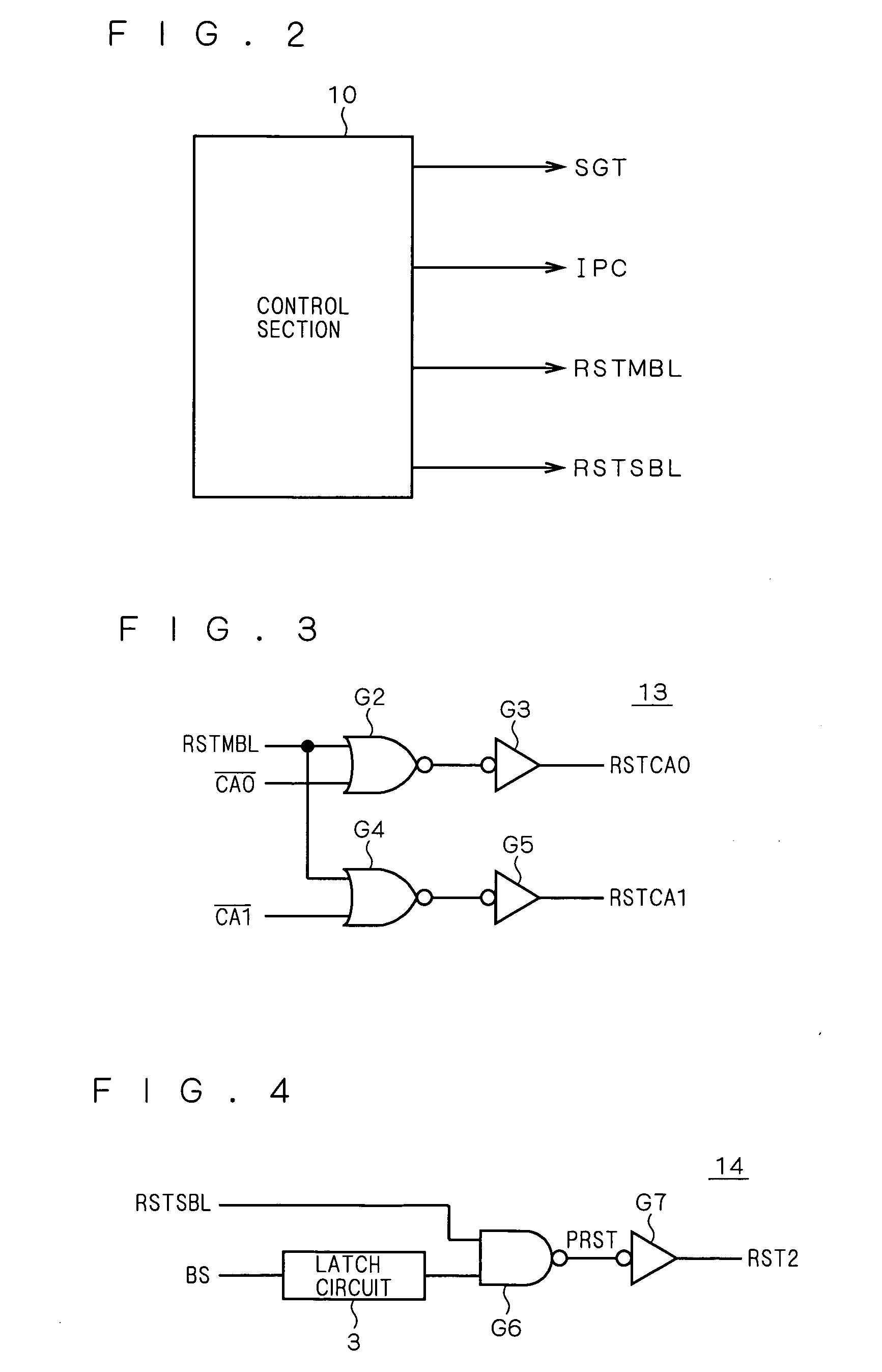
[0080] A read circuit configuration in a flash memory according to a third preferred embodiment of the present invention is the same as shown in FIG. 6 of the second preferred embodiment. The difference is the fall timing indicated by the sub-bit line selection-timing signal SGT and the rise timing indicated by the main bit line reset-timing signal RSTMBL in the control section 10 shown in FIG. 2.

[0081]FIG. 8 is a timing diagram illustrating two sequential read operations of the read circuit in the flash memory according to the third preferred embodiment. As shown, first and second read operations are sequentially performed during the read periods TR1 and TR2, in the same way as the first and second preferred embodiments.

[0082] Only the different respects from the second preferred embodiment will be explained below. The sub-bit line selection signal SG7 falls at time t11 which is delayed by a period TE from time t10 when the word line WL0, the main bit line selection signal CA1, a...


PUM


Abstract

A plurality of first sub-bit lines are each connected to a common source line via a corresponding first sub-bit line reset transistor with NMOS structure, and a plurality of second sub-bit lines are each connected to the common source line via a corresponding second sub-bit line reset transistor with NMOS structure. The plurality of first and second sub-bit line reset transistors have their respective gates receiving a sub-bit line reset signal. This sub-bit line reset signal becomes “H” for a predetermined period of time after read data is obtained during a read period.

Description

BACKGROUND OF THE INVENTION [0001] 1. Field of the Invention [0002] The present invention relates to a nonvolatile semiconductor memory device such as an electrically rewritable flash memory, and more particularly to a technique for speeding up read operation of the device. [0003] 2. Description of the Background Art [0004] A nonvolatile semiconductor memory device such as a flash memory is capable of nonvolatile storage of information by setting each of a plurality of memory transistors forming a memory cell array either to an “H” threshold voltage VthH which is a threshold value higher than read voltage, or to an “L” threshold voltage VthL which is lower than read voltage. The plurality of memory transistors are generally arranged in a matrix such that the drains (drain electrodes) thereof in each column are connected to a bit line, the gates (gate electrodes) thereof in each row are connected to a word line, and the sources (source electrodes) thereof are connected to a common so...

Claims


Application Information

Patent Timeline
IPC IPC(8): G11C16/06G11C7/06G11C7/12G11C7/18G11C11/34G11C16/24G11C16/26
CPCG11C7/062G11C7/067G11C16/26G11C7/18G11C16/24G11C7/12
Inventor OMOTO, KAYOKO
Owner RENESAS ELECTRONICS CORP
Why Eureka
Try Eureka