

Method for forming pattern using printing method
a printing method and liquid crystal display technology, applied in the field of printing methods for forming patterns in liquid crystal display panels, can solve problems such as lowering productivity, and achieve the effect of improving productivity
- Summary
- Abstract
- Description
- Claims
- Application Information
AI Technical Summary
Benefits of technology
Problems solved by technology
Method used
Image

Examples
Embodiment Construction
[0025] Reference will now be made in detail to embodiments of the present invention, examples of which are illustrated in the accompanying drawings.
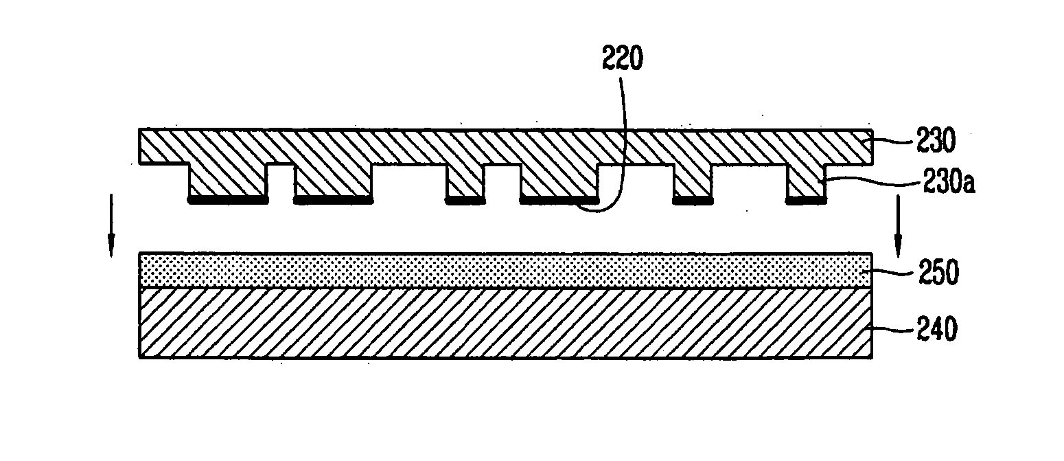
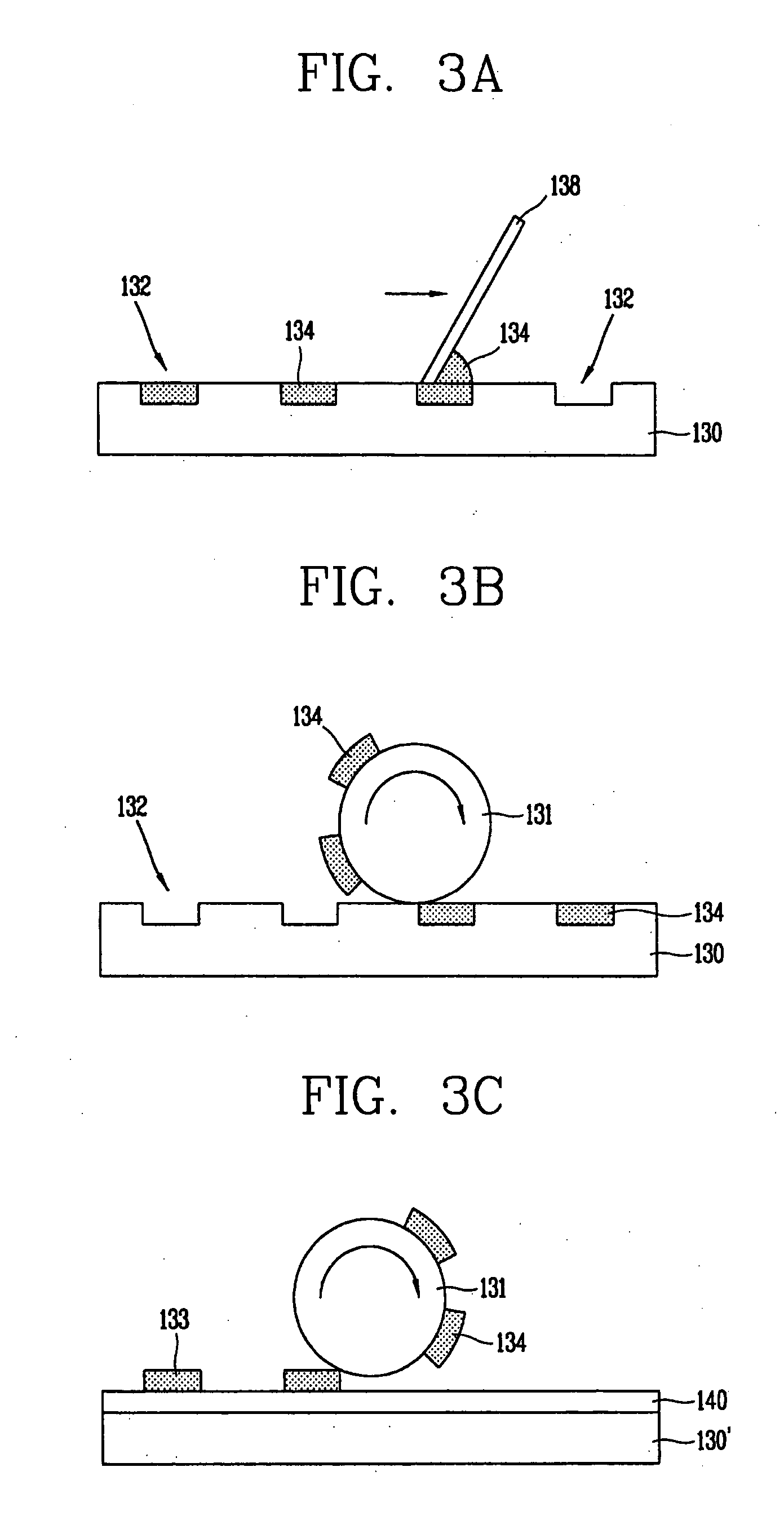
[0026] The present invention provides a printing method for forming a pattern for an active device of a display device like a liquid crystal display device. In particular, the present invention provides a gravure offset printing method in which ink is put on a concave plate, redundant ink is removed by scraping, and then printing is performed.
[0027] In gravure offset printing, since ink is transferred to a substrate using a transfer roller, the pattern can be formed with a single transfer even in display devices having large display areas because the transfer roller used corresponds to the area of the desired display device. Gravure offset printing can be used to form various patterns for the display device such as a gate line and a data line connecting with a TFT, a pixel electrode, a metal pattern for a capacitor as well as the TFT, ...
PUM
| Property | Measurement | Unit |
|---|---|---|
| adhesive force | aaaaa | aaaaa |
| thickness | aaaaa | aaaaa |
| transparent | aaaaa | aaaaa |
Abstract
Description
Claims
Application Information