Package structure of a stack-type light-sensing element and package method thereof

Inactive Publication Date: 2005-11-10
CLEAVAGE ENTERPRISE
View PDF1 Cites 6 Cited by
  • Summary
  • Abstract
  • Description
  • Claims
  • Application Information

AI Technical Summary

Benefits of technology

[0008] The primary objective of the present invention is to provide a package structure of a stack-type light-sensing element and a package method thereof, wherein a substrate, a signal-processing IC (integrated circuit) chip and a light-sensing chip are sequentially s

Problems solved by technology

However, in the aforementioned package structure of the conventional light-sensing element, the signal-processing element assembly 12 and the light-sensing unit 14 are disposed on the same plane of th

Method used


Image

  • Package structure of a stack-type light-sensing element and package method thereof
  • Package structure of a stack-type light-sensing element and package method thereof
  • Package structure of a stack-type light-sensing element and package method thereof

Examples


Embodiment Construction

[0022] To meet the requirements of current miniature electronic products, such as mobile phones, watches, portable flash memories, personal digital assistants, etc., the present invention proposes a package structure of a stack-type light-sensing element and a package method thereof in order to enable a light-sensing element to apply to miniature electronic products so that the user can carry those about conveniently.

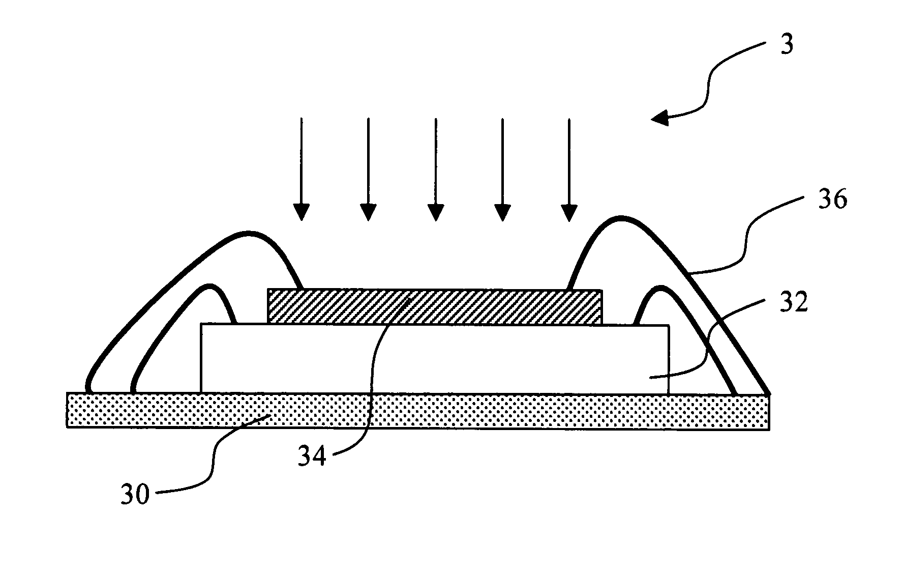
[0023] Refer to FIG. 3 a section view of the package structure of a stack-type light-sensing element according to one embodiment of the present invention, and also refer to FIG. 4 a top view of the same structure in FIG. 3. The stack-type light-sensing element 3 comprises: a substrate 30, which may be a circuit board, a metallic substrate, or a ceramic substrate; a signal-processing IC chip 32, which can amplify signal; a light-sensing chip 34, which may be made of a transparent GaN (Gallium Nitride) material or an opaque silicon material; and multiple lead lines 36, w...


PUM


Abstract

The present invention discloses a package structure of a stack-type light-sensing element and a package method thereof, wherein firstly, a substrate is provided; next, a signal-processing IC chip and a light-sensing chip are sequentially stacked above the substrate in bottom-up sequence; next, lead lines are used to electrically connect the substrate with the signal-processing IC chip and the light-sensing chip in order to form a unitary light-sensing element. The present invention has the advantages that light-sensor signals are directly processed and then output to a display device, and that the volume of a light-sensing element can be reduced to such an extent that it can be easily applied to miniature electronic products. In contrast with the conventional light-sensing element needing massive volume of electronic circuits to process signal and also needing minute and complicated assemblage, the present invention has superior novelty and futurity.

Description

BACKGROUND OF THE INVENTION [0001] 1. Field of the Invention [0002] The present invention relates to a stack-type light-sensing element, particularly to a package structure of a stack-type light-sensing element and a package method thereof, [0003] 2. Description of the Related Art [0004] Light-sensing element can be applied to alarm systems, photometers, or fire detection, biological inspection, air pollution detection devices, etc. [0005] Refer to FIG. 1 a section view of the package structure of a conventional light-sensing element, and also refer to FIG. 2 a top view of the same structure in FIG. 1. The conventional light-sensing element 1 comprises: a circuit board 10, a signal-processing element assembly 12 and a light-sensing unit 14. [0006] However, in the aforementioned package structure of the conventional light-sensing element, the signal-processing element assembly 12 and the light-sensing unit 14 are disposed on the same plane of the circuit board 10, which results in a ...

Claims


Application Information

Patent Timeline
IPC IPC(8): H01L25/18H01L27/00H01L31/0203
CPCH01L25/18H01L31/0203H01L2224/16145H01L2225/06568H01L2224/48225H01L2224/73207H01L2225/06558H01L2224/16225H01L2224/48227
Inventor HSU, CHIH-MINGLIN, CHUNG-CHENGLEE, CHIN-TING
Owner CLEAVAGE ENTERPRISE
Why Eureka
Try Eureka