Wafer and the manufacturing and reclaiming methods thereof

a technology of manufacturing and reclaiming methods, which is applied in the direction of chemical vapor deposition coating, coatings, basic electric elements, etc., can solve the problems of high cost of such methods, affecting the reclaiming rate, so as to prevent the damage to silicon substrate, increase the reclaiming rate, and increase the cost

Active Publication Date: 2005-11-10
MOSEL VITELIC INC
View PDF19 Cites 21 Cited by
  • Summary
  • Abstract
  • Description
  • Claims
  • Application Information

AI Technical Summary

Benefits of technology

[0006] Embodiments of the present invention provide a wafer and its manufacturing and reclaiming methods to overcome the shortcomings of the prior art, including high cost of the traditional reclaiming method, too many particles and brittleness on the surface of the reclaimed wafer, or discolor phenomena and surface roughness, so as to prevent the damage to silicon substrate in the reclaiming process of the wafer and to increase the reclaiming rate.
[0008] The features of the present invention include: 1) preventing the thinness and breakability of the wafer due to the reclaiming process, 2) prolonging the use-span of the wafer, 3) reducing the limit of the use of machines, and 4) other improvements as described below.

Problems solved by technology

For example, Chemical Mechanical Polish (CMP) can be used to directly remove a deposition layer (e.g., polysilicon layer); however, the cost of such method is high (because the slurry is usually expensive), and the thickness of the wafer, will become thinner through the long-term use of this method, and furthermore, the wafer may be broken due to the mechanical stress in the polishing process.
However, the materials used to remove the polysilicon layer may etch the silicon substrate as well, so that the damage to the silicon wafer occurs, and thus the reclaimed wafer will not be suitable for use as a control wafer or a dummy wafer.
Moreover, if the availability of the etching and polishing machines is limited, the used wafers cannot be reclaimed as control wafers or dummy wafers immediately, so the manufacturers need to additionally buy new wafers in response thereto.

Method used


Image

  • Wafer and the manufacturing and reclaiming methods thereof
  • Wafer and the manufacturing and reclaiming methods thereof
  • Wafer and the manufacturing and reclaiming methods thereof

Examples


Embodiment Construction

[0012] Some typical embodiments to present the features and advantages of the present invention will be particularly described in the following illustrations. It should be understood that the present invention may have various modifications in different modes, which are not apart from the scope of the present invention, and the illustrations and drawings of the present invention are substantially used for explaining but not for limiting the present invention.

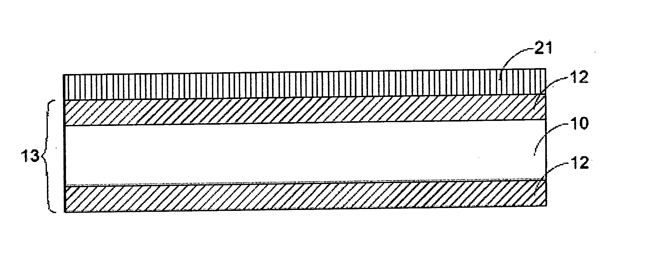
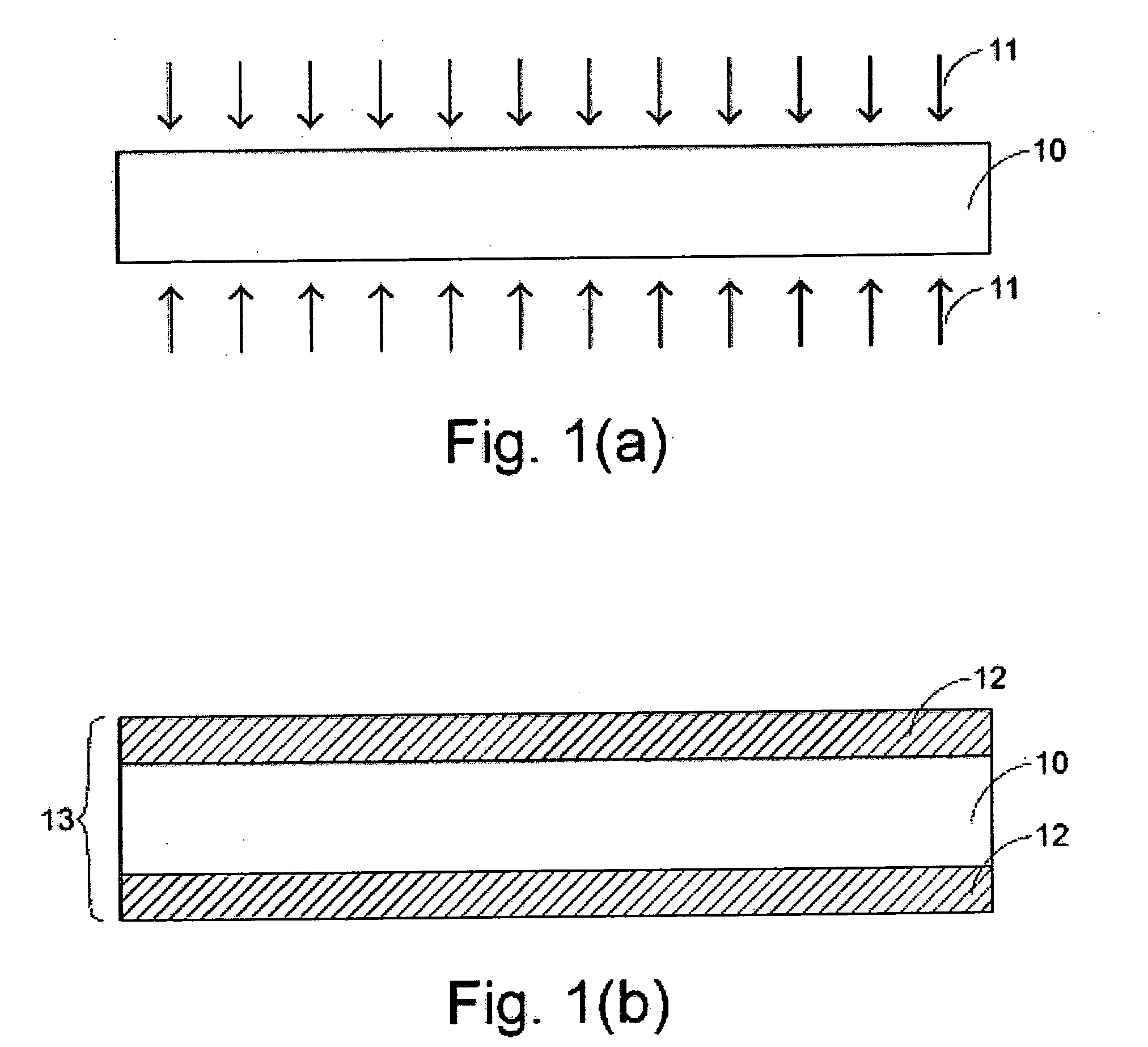
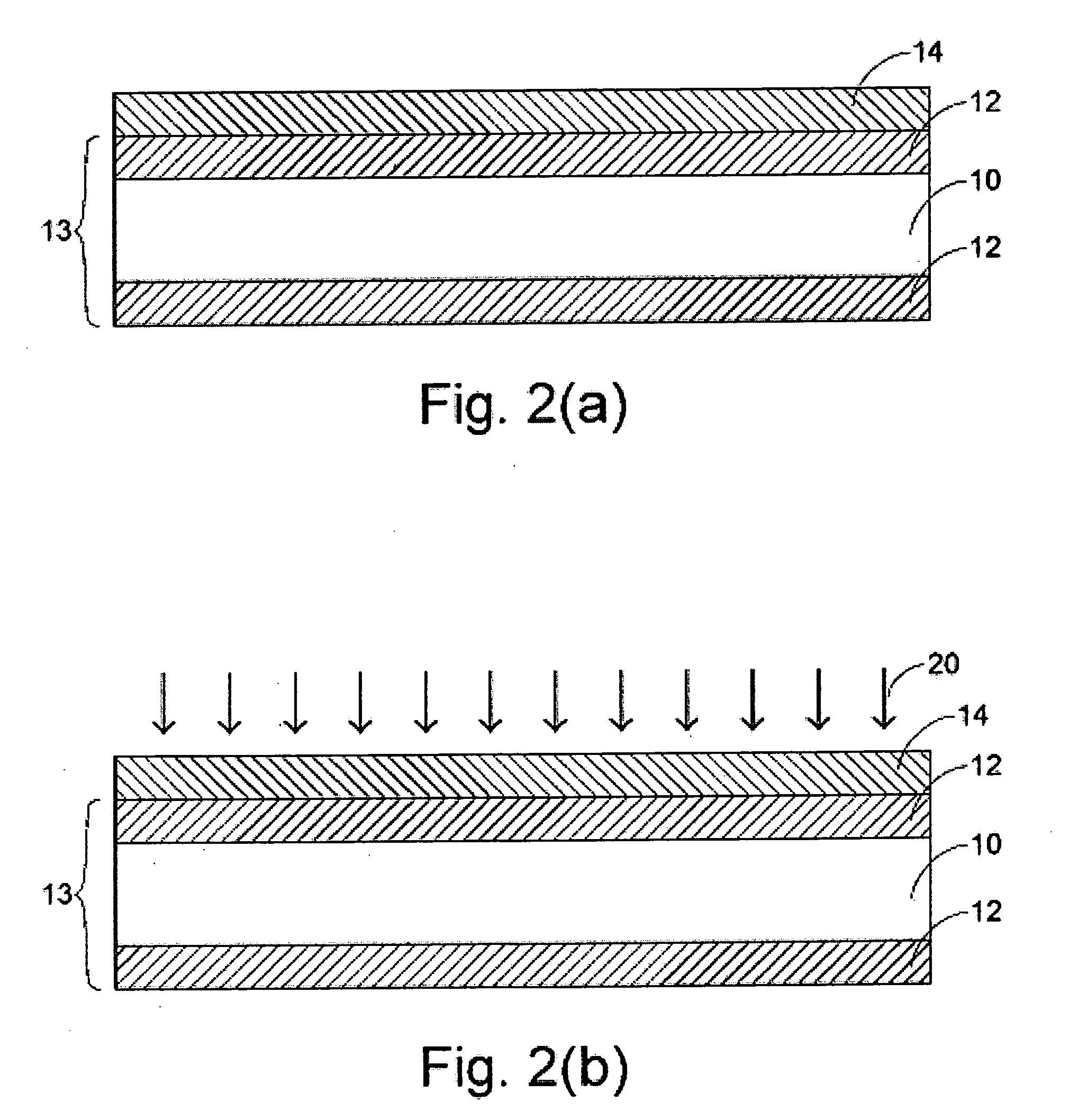
[0013] The wafer provided by embodiments of the present invention is applied in electronic component fabrication to improve the quality of the deposition process (e.g., polysilicon deposition process). The wafer can be considered as the control wafer or the dummy wafer. For example, the wafer can be put into the furnace together with the wafer for productive purposes to process the polysilicon deposition. Thereby, according to the thickness of polysilicon deposited on the control wafer, the stability of fabrication can be contr...


PUM

PropertyMeasurementUnit
pressureaaaaaaaaaa
pressureaaaaaaaaaa
operative temperatureaaaaaaaaaa

Abstract

A wafer and the manufacturing and reclaiming methods thereof are disclosed. The wafer includes a semiconductor substrate and a protective layer formed on the surface of the semiconductor substrate. The reclaiming method of the wafer includes providing a wafer having a semiconductor substrate, a protective layer formed on the semiconductor substrate, and a polysilicon layer formed on the protective layer; and removing the polysilicon layer. The wafer and the reclaiming method of the wafer can prevent the substrate of the wafer from being destroyed during the reclaiming process and increase the reclaiming rate of the wafer.

Description

CROSS-REFERENCES TO RELATED APPLICATIONS [0001] This application claims priority from R.O.C. Patent Application No. 093113073, filed May 10, 2004, the entire disclosure of which is incorporated herein by reference. BACKGROUND OF THE INVENTION [0002] The present invention relates to a wafer and manufacturing and reclaiming methods of the wafer, and more particularly to a control wafer or a dummy wafer and the manufacturing and reclaiming methods thereof. [0003] In the semiconductor industry, the wafer for controlling the semiconductor fabrication is called a control wafer, and the wafer for maintaining the stability of single-batch fabrication is called a dummy wafer. For example, during the polysilicon deposition process in a furnace, the wafer for non-productive purposes (e.g., control wafer) and the wafer for productive purposes are put into the boat together to control the stability of batch-to-batch fabrication by measuring the thickness of the polysilicon deposited on the wafer...

Claims


Application Information

Patent Timeline
Patent Type & Authority Applications(United States)
IPC IPC(8): H01L21/00H01L21/02H01L21/46H01L23/58
CPCH01L21/02079H01L21/02032
Inventor CHANG, JEN CHIEHCHUNG, YI FUSUN, PEI-FENG
Owner MOSEL VITELIC INC
Why Eureka
Try Eureka