Electroluminescent device

a technology of electroluminescent devices and substrates, applied in thermoelectric devices, identification means, instruments, etc., can solve problems such as poor light generation efficiency, and achieve the effect of fast rise and fall times and fast operation

Inactive Publication Date: 2005-11-17
SHARP KK
View PDF8 Cites 24 Cited by
  • Summary
  • Abstract
  • Description
  • Claims
  • Application Information

AI Technical Summary

Benefits of technology

[0009] The present invention is able to generate light, from a sub-micron to many micron-sized devices, on a silicon wafer. Advantageously, the emitted light has a wavelength between 350 nanometers (nm) and 700 nm, which is near the UV and visible regions of the spectrum, and predominantly in the wavelength between 370 and 390 nm. As the EL device is formed on a Si substrate, it can be fabricated using many of

Problems solved by technology

For silicon devices, the light generation efficiency is known to be poor and the photon energy is predominantly around 2 eV.
However, these devices ar

Method used


Image

  • Electroluminescent device
  • Electroluminescent device
  • Electroluminescent device

Examples


Embodiment Construction

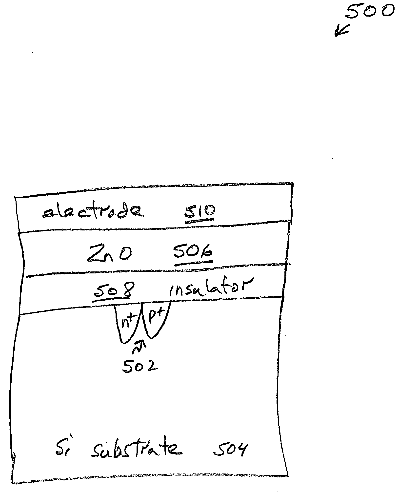
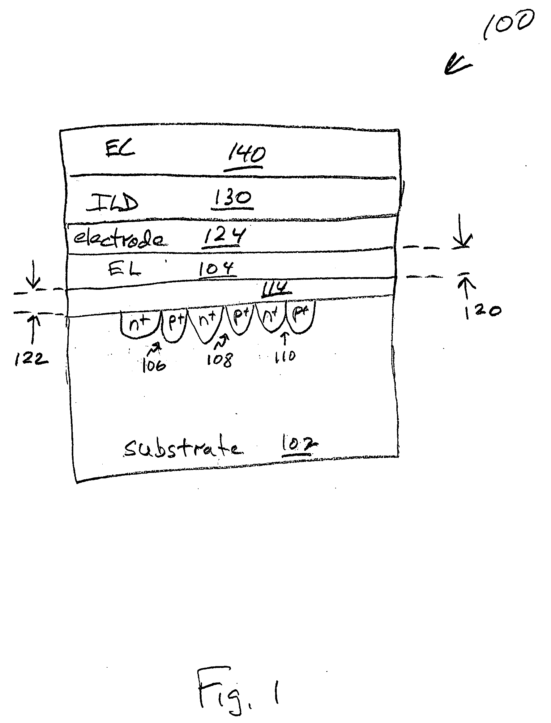
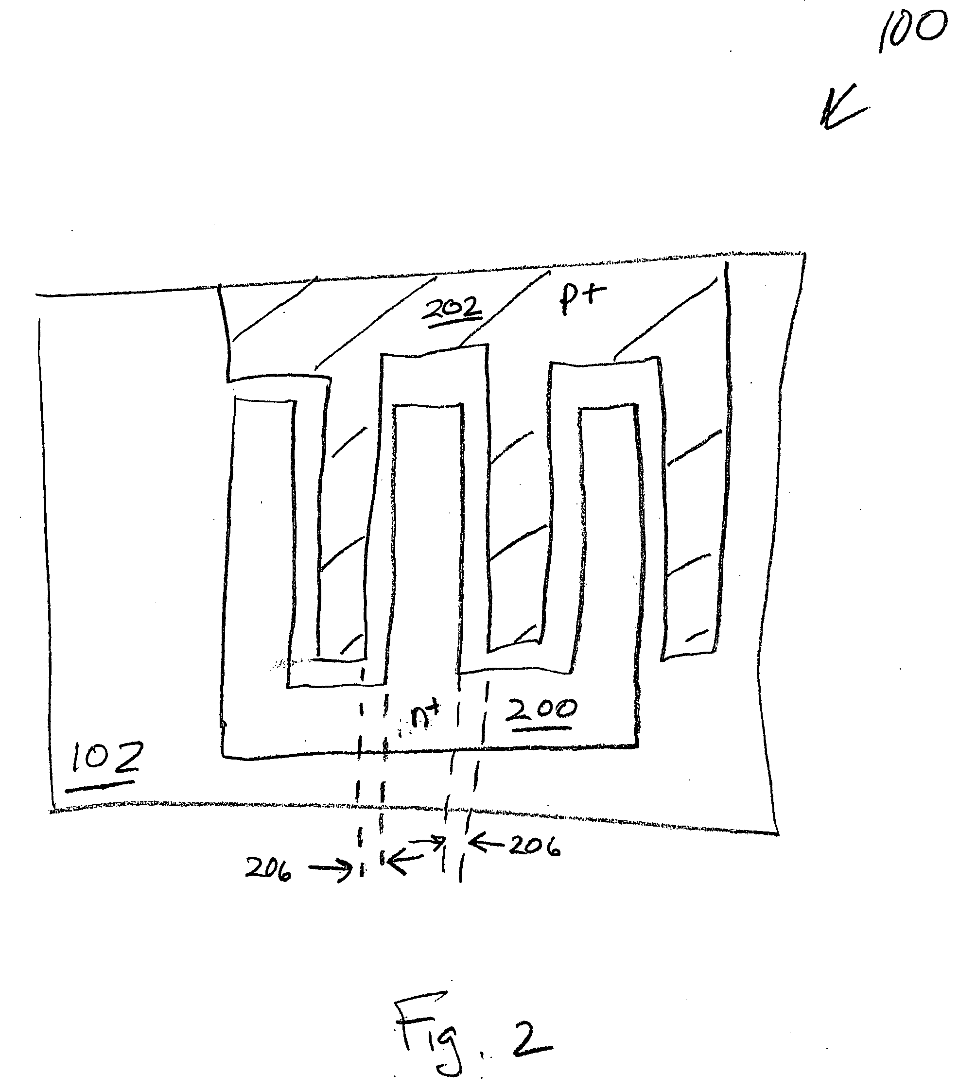
[0032]FIG. 3 is a partial cross-sectional view of a first aspect of the present invention electroluminescent device. As an alternative to the explanation of FIG. 1 (explained below), the device 300 may be understood, in its simplest form, to comprise a p+ / n+ junction 302 and an electroluminescent layer 304 overlying the p+ / n+ junction 302. As in FIG. 1 the p+ / n+ junction 302 may be formed in a type IV semiconductor material substrate 306. It should be noted that the p+ / n+ junction may be formed in other types of substrate materials, besides type IV materials. The type IV substrate materials are cited because of their use in conventional CMOS processes.

[0033] The type IV semiconductor material 306 can be Si, C, Ge, SiGe, and SiC. For example, SOI, bulk Si, Si on glass, and Si on plastic substrates may be used. Again, as in FIG. 1, the electroluminescent layer 304 is a material such as nanocrystalline Si, nanocrystalline Ge, fluorescent polymers, or type II-VI materials such as ZnO, ...


PUM


Abstract

A method is provided for forming an electroluminescent device. The method comprises: providing a type IV semiconductor material substrate; forming a p+/n+ junction in the substrate, typically a plurality of interleaved p+/n+ junctions are formed; and, forming an electroluminescent layer overlying the p+/n+ junction(s) in the substrate. The type IV semiconductor material substrate can be Si, C, Ge, SiGe, or SiC. For example, the substrate can be Si on insulator (SOI), bulk Si, Si on glass, or Si on plastic. The electroluminescent layer can be a material such as nanocrystalline Si, nanocrystalline Ge, fluorescent polymers, or type II-VI materials such as ZnO, ZnS, ZnSe, CdSe, and CdS. In some aspect, the method further comprises forming an insulator film interposed between the substrate and the electroluminescent layer. In another aspect, the method comprises forming a conductive electrode overlying the electroluminescent layer.

Description

BACKGROUND OF THE INVENTION [0001] 1. Field of the Invention [0002] This invention generally relates to integrated circuit (IC) fabrication and, more particularly, to a direct current (dc), type IV substrate electroluminescent device and corresponding fabrication processes. [0003] 2. Description of the Related Art [0004] The generation of light from semiconductor devices is possible, regardless of whether the semiconductor material forms a direct or indirect bandgap. High field reverse biased p-n junctions create large hot carrier populations that recombine with the release of photons. For silicon devices, the light generation efficiency is known to be poor and the photon energy is predominantly around 2 eV. The conversion of electrical energy to optical photonic energy is called electroluminescence (EL). Efficient EL devices have been made that can operate with small electrical signals, at room temperature. However, these devices are fabricated on materials that are typically not c...

Claims


Application Information

Patent Timeline
IPC IPC(8): G09F9/00H01L27/32G09F9/30H01L29/08H01L33/18H01L33/28H01L33/34H01L35/24
CPCH01L33/18Y10S977/95H01L33/34H01L33/28
Inventor ONO, YOSHIGAO, WEICONLEY, JOHN F. JR.NISHIO, OSAMUSAKIYAMA, KEIZO
Owner SHARP KK
Why Eureka
Try Eureka