Semiconductor light emitting device and method of manufacturing the same

a semiconductor technology, applied in the direction of semiconductor devices, basic electric elements, electrical equipment, etc., can solve the problems of lowering the wavelength conversion efficiency in higher temperatures, lowering the wavelength conversion efficiency, etc., to improve the appearance of the semiconductor light emitting device, the effect of lowering the temperature at the fluorescent material

Inactive Publication Date: 2005-11-17
STANLEY ELECTRIC CO LTD
View PDF17 Cites 43 Cited by
  • Summary
  • Abstract
  • Description
  • Claims
  • Application Information

AI Technical Summary

Benefits of technology

[0014] Thus, the wavelength conversion spacer can be retained at almost the same temperature overall. If a part of this spacer is brought to a high temperature, that part lowers the conversion efficiency to cause a partially dark portion that leads to the so-called color variation. Such color variation worsens the ...

Problems solved by technology

The fluorescent material can not convert all the impinged blue light into yellow light, but has the tendency to lower the wavelength conversion efficiency as the density of t...

Method used


Image

  • Semiconductor light emitting device and method of manufacturing the same
  • Semiconductor light emitting device and method of manufacturing the same
  • Semiconductor light emitting device and method of manufacturing the same

Examples


Embodiment Construction

[0022] The invention will now be described in detail based on the exemplary embodiments shown in the drawings. In these figures, identical or similar members are labeled using the same symbols, and in some cases, descriptions of these common members are omitted. Although the following embodiments are exemplary of the invention, the invention is in no way limited to the embodiments presented below.

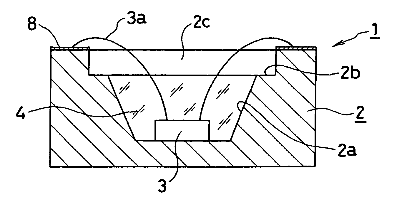
[0023]FIGS. 1-2 show a base 2, which can be employed to form a semiconductor light emitting device 1 made in accordance with the principles of the invention. A first cavity 2a can be formed as a substantially conical recess in the base 2. An LED chip 3 such as a blue light emitting source can be die-mounted in the cavity, and a transparent resin spacer 4 can be filled therein and can have a goal of providing humidity protection around the LED chip 3.

[0024] A second cavity 2c can be formed above the first cavity 2a. The second cavity 2c can have a larger diameter than the maximum diameter ...


PUM


Abstract

A semiconductor light emitting device can include a base having a cavity provided for housing an LED chip and a resin spacer therein. The resin spacer can be composed of at least two layers of spacers including a transparent resin spacer and a wavelength conversion spacer mixed with a fluorescent material and formed to have an almost constant thickness. The wavelength conversion spacer can include a metallic radiation mesh or radiation wire disposed therein.

Description

[0001] This application claims the priority benefit under 35 U.S.C. §119 of Japanese Patent Application No. 2004-128152 filed on Apr. 23, 2004, which is hereby incorporated by reference. BACKGROUND OF THE INVENTION [0002] 1. Field of the Invention [0003] The invention relates to an LED lamp and method of manufacture, and more particularly to a structure of the so-called white LED lamp that includes an LED chip capable of emitting a blue light. A fluorescent material can be disposed on or adjacent to an optical path of the light emitted from the LED chip to emit a yellow light when excited by the blue light. The blue light from the LED chip and the yellow light from the fluorescent material can be mixed to yield a white light, which can then be externally emitted. [0004] 2. Description of the Related Art [0005] An LED chip capable of emitting a blue light, and a fluorescent material that is operative to emit a yellow light when excited by the blue light from the LED chip, are employe...

Claims


Application Information

Patent Timeline
IPC IPC(8): H01L33/50H01L33/54H01L33/56H01L33/64
CPCH01L33/486H01L33/507H01L2924/3025H01L2924/19107H01L24/45H01L2224/45147H01L2224/45144H01L2224/45124H01L2224/48091H01L33/644H01L2924/00014H01L2924/00
Inventor HARADA, MITSUNORI
Owner STANLEY ELECTRIC CO LTD
Why Eureka
Try Eureka