Chip embedded package structure

Active Publication Date: 2005-11-17
VIA TECH INC
View PDF9 Cites 61 Cited by
  • Summary
  • Abstract
  • Description
  • Claims
  • Application Information

AI Technical Summary

Benefits of technology

[0013] Accordingly, the present invention is directed to a chip embedded package structure capable of shortening the processi

Problems solved by technology

The tape needs to be torn away and the surface needs to be cleaned so that the process is complicated but trivial.
Moreover, after tearing the tape away from the chip and the stiffener, coplanarity between the chip and the stiffener is hard to maintain.
Ultimately, this may reduce the reliability of the subsequently formed multi

Method used


Image

  • Chip embedded package structure
  • Chip embedded package structure
  • Chip embedded package structure

Examples


Example

[0021] Reference will now be made in detail to the present preferred embodiments of the invention, examples of which are illustrated in the accompanying drawings. Wherever possible, the same reference numbers are used in the drawings and the description to refer to the same or like parts.

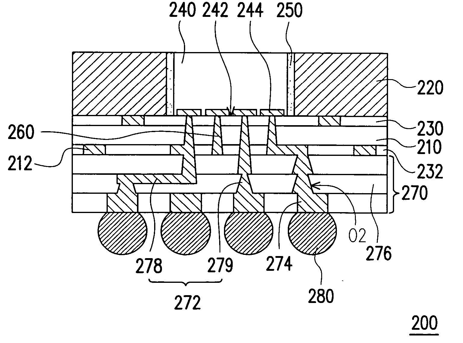
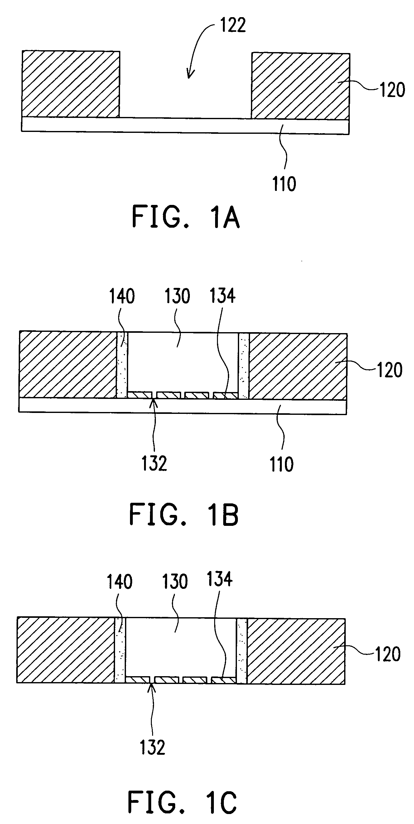
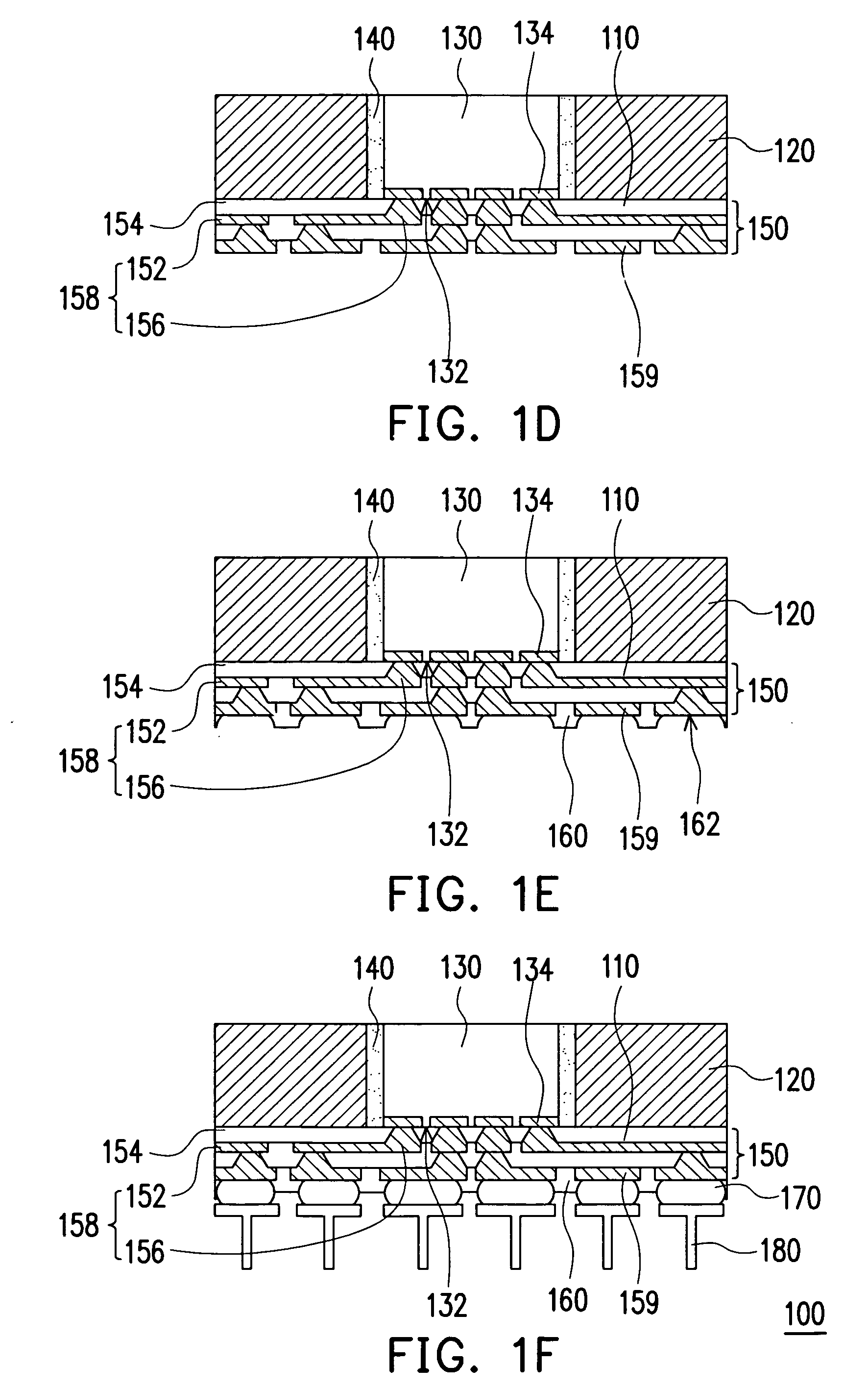
[0022]FIGS. 2A through 2G are schematic cross-sectional views showing the steps of fabricating a chip embedded package structure according to one embodiment of the present invention. First, as shown in FIG. 2A, a tape 210 is provided. The tape 210 is a polyimide (PI) tape, for example. The tape 210 comprises at least an alignment mark 212 (four alignment marks in the illustration) on the surface of the tape 210. These alignment marks 212 are not limited to any one side of the tape 210. In general, the alignment marks 212 can be disposed on both sides of the tape 210.

[0023] The tape 210 may further comprise a circuit layer 216 disposed on a surface that will not come in contact with a subsequently ...


PUM


Abstract

A chip embedded package structure is provided. A stiffener is disposed on a tape. The tape has at least an alignment mark and the stiffener has at least a chip opening. A chip having a plurality of bonding pads thereon is disposed on the tape within the chip opening such that the bonding pads face the tape. A plurality of through holes is formed in the tape to expose the bonding pads respectively. After that, an electrically conductive material is deposited to fill the through holes and form a plurality of conductive vias that connects with the bonding pads respectively. A multi-layered interconnection structure is formed on the surface of the tape away from the chip. The multi-layered interconnection structure has an inner circuit that connects to the conductive vias. The inner circuit has a plurality of metallic pads disposed on the outer surface of the multi-layered interconnection structure.

Description

CROSS-REFERENCE TO RELATED APPLICATION [0001] This application claims the priority benefit of Taiwan application serial no. 93113134, filed on May 11, 2004. BACKGROUND OF THE INVENTION [0002] 1. Field of the Invention [0003] The present invention relates to a chip package structure. More particularly, the present invention relates to a chip embedded package structure. [0004] 2. Description of Related Art [0005] In this electronic age, multi-functional, highly integrated, miniaturized, inexpensive devices with a high processing speed are in great demand. To meet this trend, chip packages are also highly miniaturized and densified. In the conventional ball grid array (BGA) packaging technique, a package substrate is often used as a carrier for an integrated circuit (IC) chip. The chip disposed over the package substrate is electrically connected to the substrate through flip chip bonding or wire bonding. An array of solder balls is also attached to the bottom surface of the package su...

Claims


Application Information

Patent Timeline
IPC IPC(8): H01L23/31H01L23/48H01L23/538H01L23/544
CPCH01L21/6835H01L2224/16235H01L23/544H01L2223/54473H01L2224/04105H01L2224/20H01L2924/14H01L2924/15174H01L2924/15311H01L2924/15312H01L2924/18162H01L2924/01033H01L24/19H01L2224/0401H01L23/5389H01L2224/12105H01L2224/32225H01L2224/83132H01L2224/92144H01L2924/12042
Inventor CHANG, WEN-YUAN
Owner VIA TECH INC
Why Eureka
Try Eureka