

Method and structure for improving adhesion between intermetal dielectric layer and cap layer
a dielectric layer and cap layer technology, applied in the direction of semiconductor devices, semiconductor/solid-state device details, electrical apparatus, etc., can solve the problems of poor adhesion between the low-k material and its neighboring structures or layers, high thermal expansion rate, and low thermal conductivity relative to neighboring structures and layers, so as to reduce excessive stress and eliminate delamination
- Summary
- Abstract
- Description
- Claims
- Application Information
AI Technical Summary
Benefits of technology
Problems solved by technology
Method used
Image

Examples
Embodiment Construction
[0019] Referring now to the drawings, wherein like reference numbers are used herein to designate like or similar elements throughout the various views, illustrative embodiments of the present invention are shown and described. The figures are not necessarily drawn to scale, and in some instances, the drawings have been exaggerated and / or simplified in places for illustrative purposes only. One of ordinary skill in the art will appreciate the many possible applications and variations of the present invention based on the following illustrative embodiments of the present invention.
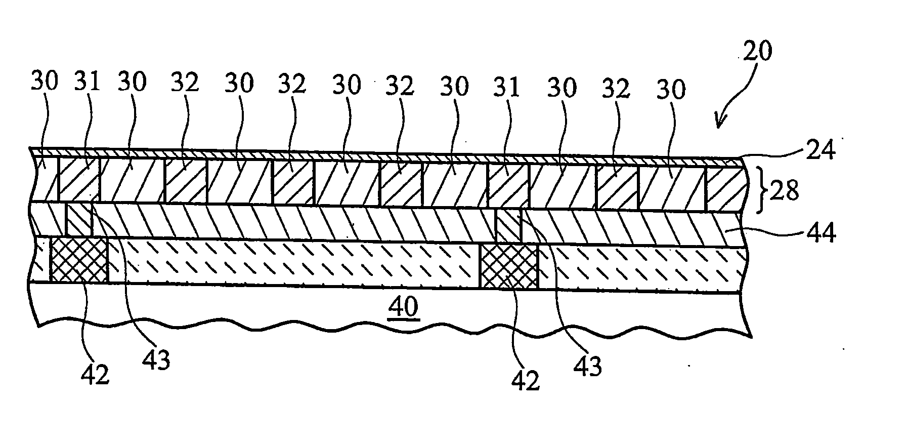
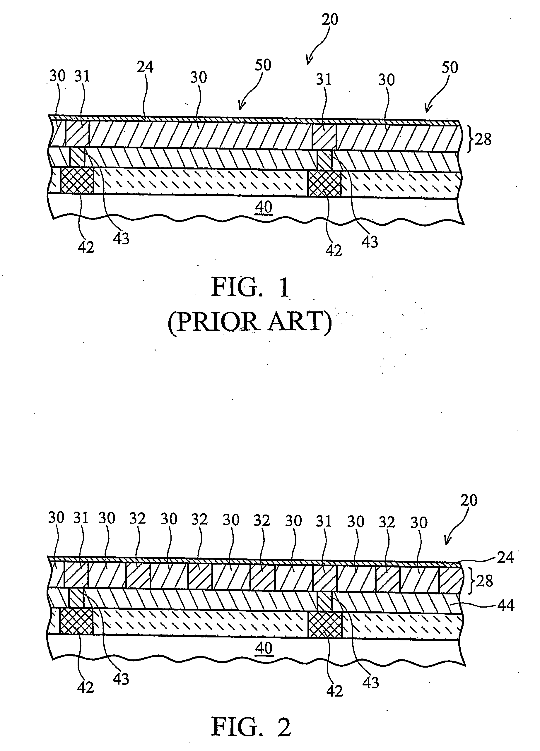
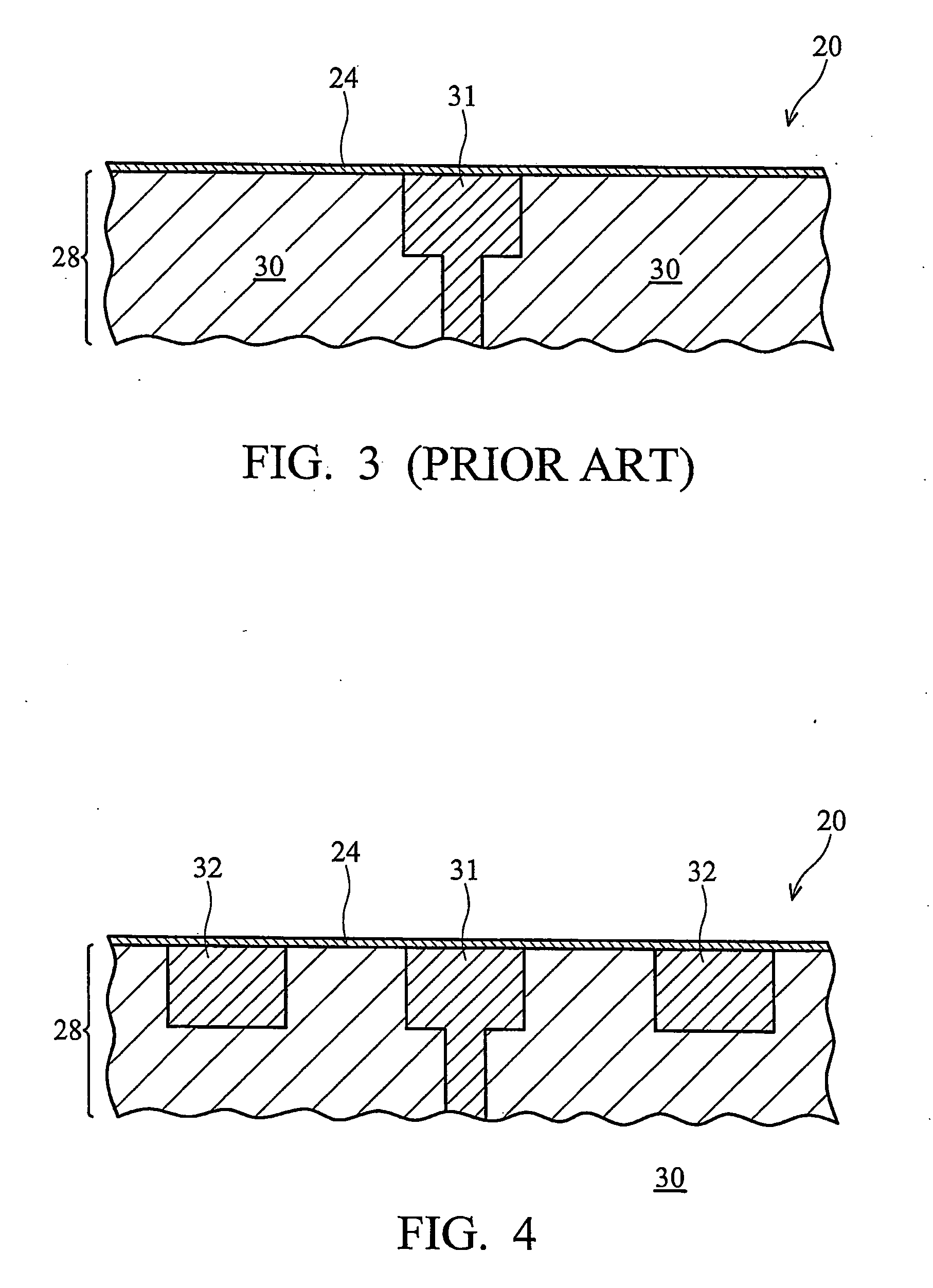
[0020] Generally, an embodiment of the present invention provides a scheme and method of improving adhesion between an IMD (inter-metal dielectric) layer and a cap layer in contact therewith in a semiconductor interconnect structure. FIG. 2 is a cross-section view for part of a semiconductor interconnect structure 20 for a first embodiment of the present invention. The interconnect structure 20 of FIG. 2 i...
PUM
 Abstract
Description
Claims
Application Information