
Semiconductor device

a technology of semiconductor devices and semiconductor films, applied in semiconductor devices, semiconductor/solid-state device details, electrical apparatus, etc., can solve the problems of low mechanical strength and hardness of the insulation film, and the film itself is peeled off or broken by impact, etc., to achieve great merit for the industry

Inactive Publication Date: 2005-11-17
NEC ELECTRONICS CORP
View PDF6 Cites 7 Cited by
  • Summary
  • Abstract
  • Description
  • Claims
  • Application Information

AI Technical Summary

Benefits of technology

[0043] According to the invention, a semiconductor device which is resistant to failure even when less strong insulating material having less compact film structure or insulating material prone to peeling off when stacked is used and a characteristic test is performed by probing the interconnect structure in the course of fabricating it into the semiconductor substrate or bonding to the pad is performed, and thus, the merit on industry is great.

Problems solved by technology

However, these insulating films have low mechanical strength and hardness.
A problem is that in a probe test for operation check before shipment, the film itself is peeled off or broken by mechanical impact transmitted from the probe needle.
Another problem is that the film itself is peeled off or broken by impact due to vibration and load applied during bonding wires for retrieving electrical signals from or supplying power to the semiconductor chip.
For this reason, in the process after the semiconductor substrate is diced into chips, insulating material may allow moisture or corrosive gas to intrude from the exposed side surface of the chip, which leads to the cause of disconnection failure by corroding metal interconnects serving as signal lines or power supply lines in the semiconductor chip.
However, after independent investigation, the inventor has found that there still remain problems that cannot be avoided by the structures described above.
However, the inventor has found that there occur problems that cannot be avoided by implementing a simple collection of such ideas.
This results in a problem of intrusion of moisture or corrosive gas, which leads to the cause of disconnection failure by corroding metal interconnects serving as signal lines or power supply lines in the semiconductor chip.
Furthermore, also during wire bonding, there is a risk that a crack 1701 may be produced in the top interconnect layer to expose insulating material directly below the interconnect layer.
This results in a problem of causing similar failure.
On the other hand, as illustrated in FIG. 14, when the structure of embedding metal film entirely (see the first and second patent documents) is used, the fabrication process is complicated if the metal film is embedded later in the pad portion.
This causes a problem of “dishing”, that is, reduced thickness of the metal interconnect below the pad.
In fact, large unevenness occurs in the same layer, which causes the risk of peeling off or defocusing in the exposure process, thus making it difficult to fabricate a desired semiconductor device.
In addition, as illustrated in FIG. 15, the method of directly bonding the underlying conducting layer (see the first and second patent documents) involves a complicated fabrication process and increases the area occupied by the pad portion.
Therefore this method is disadvantageous for downscaling of semiconductor chips.
As described above, when less strong insulating material having less compact film structure or insulating material prone to peeling off when stacked is used and a characteristic test is performed by probing the interconnect structure in the course of fabricating it into the semiconductor substrate or bonding to the pad is performed, it is a challenging problem to avoid exposure of the insulating material having less compact film structure.
In particular, it is very difficult to fabricate devices, which must meet future demands for further downscaling, without using complicated processes.

Method used


Image

  • Semiconductor device
  • Semiconductor device
  • Semiconductor device

Examples


first embodiment

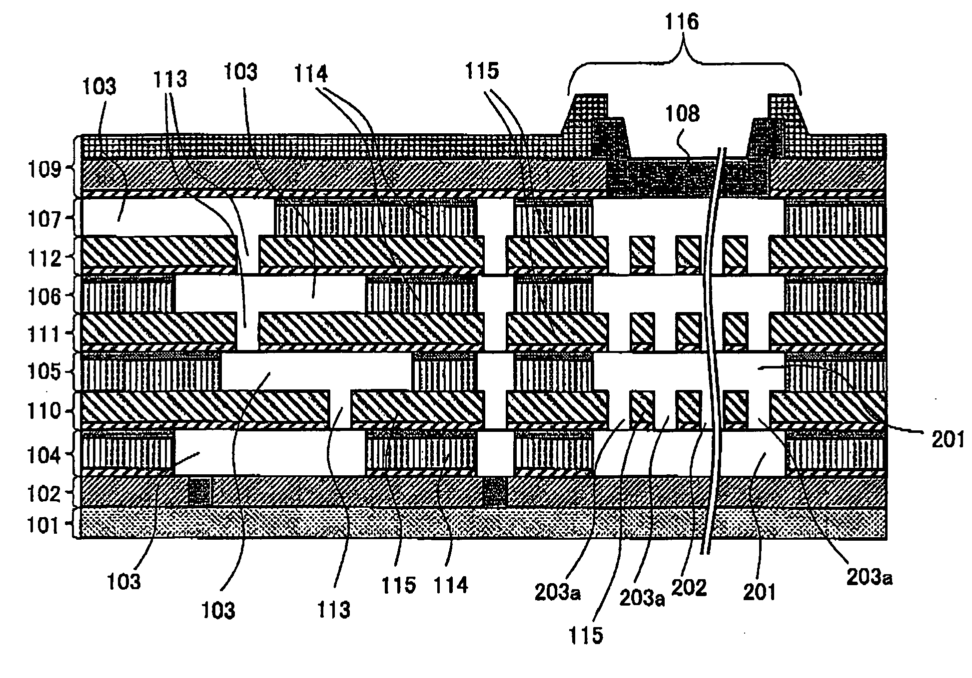
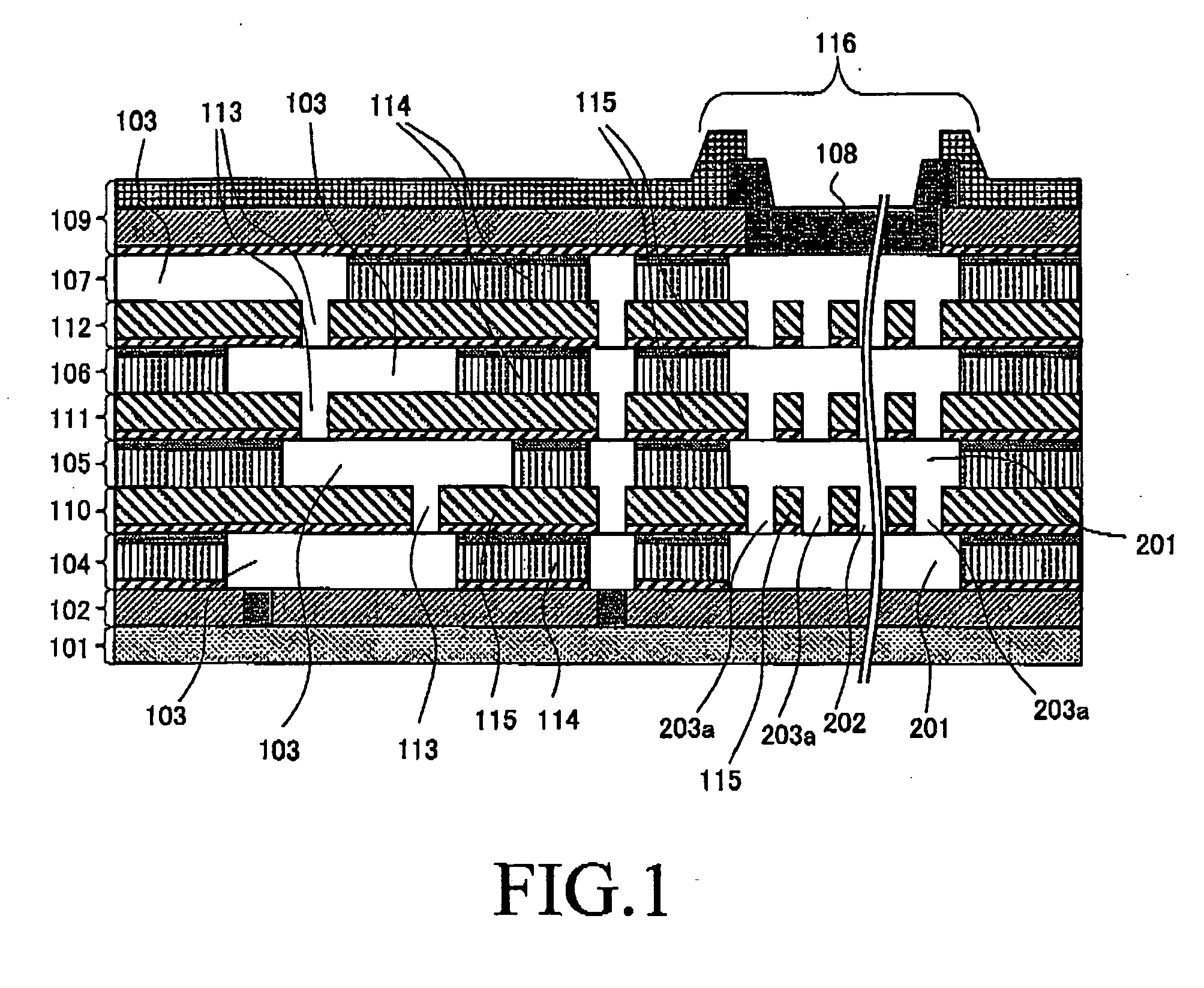
[0064]FIG. 1 is a cross-sectional view showing a semiconductor device according to an embodiment of the invention.

[0065] More specifically, the semiconductor device comprises a front end layer 101 in which diffusion layers, gate electrodes, and transistors are formed on a semiconductor substrate. The front end layer 101 is covered, across a contact plug layer 102, sequentially with interconnect layers 104, 105, 106, and 107 including interconnects 103 provided for connection in the same layer. On top, adhesion / barrier metal, pad connecting aluminum (Al) 108, and a passivation layer 109 are placed. The region below the pad connecting aluminum 108 will be referred to as “subpad region”, and the other region as “extrapad region”.

[0066] It should be noted that in an actual semiconductor device, a predetermined number of interconnect layers and via layers are repeatedly stacked to form a multilayer interconnect. However, it is omitted in FIG. 1 for simplicity.

[0067] In this semiconduc...

second embodiment

[0085] Next, the second embodiment of the invention will be described.

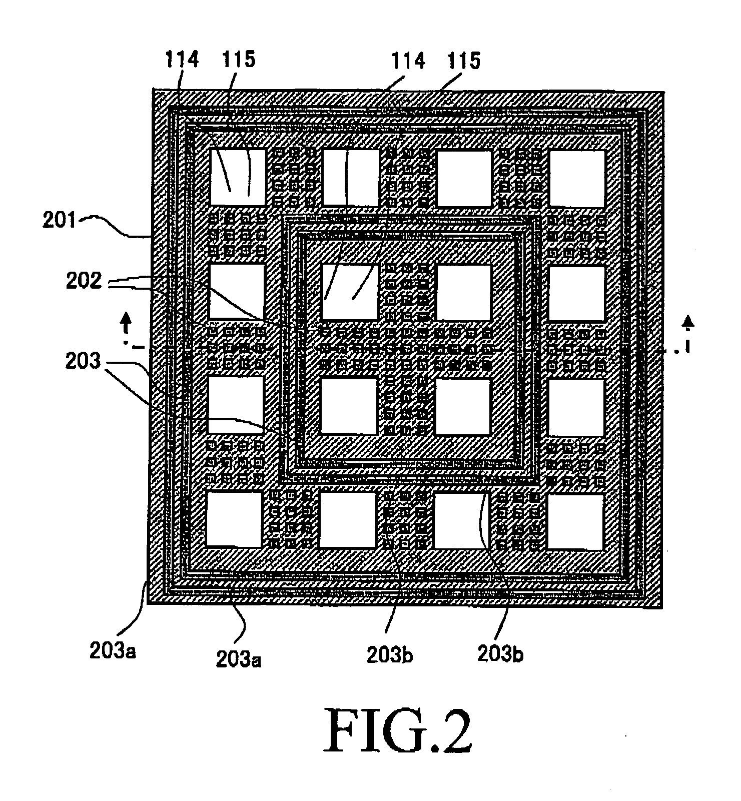
[0086]FIG. 10 is a perspective plan view illustrating the planar structure of a relevant part of a semiconductor device according to this embodiment.

[0087] More specifically, in this specific example, a plurality of bonding pads are located around the chip. A plurality of loop-shaped chip periphery metal interconnects 1002 are located along the periphery of the chip so as to surround the inside 1001 of the chip including subpad regions 116 underlying these bonding pads. The chip periphery metal interconnect 1002 is provided for all the layers including low-k insulating material.

[0088]FIG. 11 is a schematic view showing a cross-sectional structure of each chip periphery metal interconnect 1002.

[0089] The interconnect layers 104, 105, 106, and 107 are provided with interconnects 1101, respectively. The via layers 110, 111, and 112 are provided with interconnect layers 1102, respectively. In addition, each of the...


PUM


Abstract

A semiconductor device comprises a semiconductor layer; a stacked body; and an electrode pad provided on the stacked body. The stacked body is provided on the semiconductor layer and has a plurality of stacked layers. The electrode pad is provided on the stacked body. The stacked body has a subpad region that is located below the electrode pad and an extrapad region that is not located below the electrode pad, and any portion made of insulating material in the electrode subpad region except a contact plug layer directly above the semiconductor layer in the stacked body is surrounded by a metal interconnect having a closed structure in the same layer.

Description

CROSS-REFERENCE TO ERLATED APPLICATIONS [0001] This application is based upon and claims the benefit of priority from the prior Japanese Patent Application No. 2004-141835, filed on May 12, 2004; the entire contents of which are incorporated herein by reference. BACKGROUND OF THE INVENTION [0002] The invention relates to a semiconductor device, and more particularly, to a semiconductor device resistant to occurrence of failure even if it is made of less strong insulating material having less compact film structure or insulating material prone to peeling off when stacked. [0003] In recent years, in order to address requests for downscaling and speed enhancement of semiconductor devices, not only the scaling of transistors fabricated in the semiconductor substrate surface but also the scaling of interconnect layer portions connecting between the transistors have been indispensable. When an interconnect layer portion is scaled down, the product RC of the resistance R of the interconnec...

Claims


Application Information

Patent Timeline
Patent Type & Authority Applications(United States)
IPC IPC(8): H01L21/60H01L23/12H01L21/768H01L23/485H01L23/528H01L27/14
CPCH01L24/05H01L24/48H01L2924/01033H01L2924/01023H01L2924/01019H01L2924/00014H01L2924/3025H01L2224/02166H01L2224/04042H01L2224/05093H01L2224/05556H01L2224/05558H01L2224/05624H01L2224/48463H01L2924/01004H01L2924/01005H01L2924/01006H01L2924/01013H01L2924/01014H01L2924/01029H01L2924/01058H01L2924/01079H01L2924/01082H01L2924/30105H01L2224/45099H01L2224/05554
Inventor TSUDA, HIROSHI
Owner NEC ELECTRONICS CORP
Learn More